PV-Tools TLM-SCAN Contact Resistivity Mapping System
| Brand | PV-Tools |
|---|---|
| Origin | Germany |
| Manufacturer Type | Authorized Distributor |
| Origin Category | Imported |
| Model | TLM-SCAN |
| Pricing | Available Upon Request |
Overview
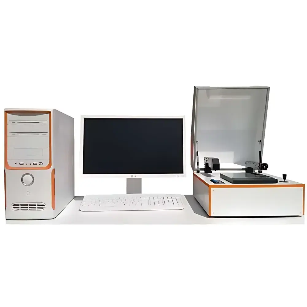
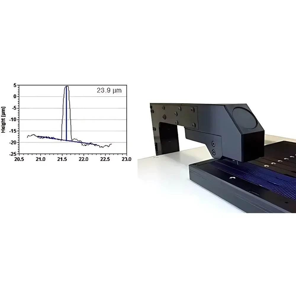
The PV-Tools TLM-SCAN is a fully motorized, high-precision contact resistivity mapping system engineered for spatially resolved characterization of front-side metallization on crystalline silicon solar cells and test structures. It implements the Transmission Line Method (TLM), a physically rigorous, four-point-probe-based technique standardized in photovoltaic process development (e.g., ASTM F1529, IEC 60904-10). Unlike conventional single-point TLM measurements, the TLM-SCAN acquires quantitative maps of specific contact resistivity (ρc, unit: mΩ·cm²), finger line resistance (Rsheet), finger width (Wf), and—when integrated with optional surface profilometry—finger height (Hf). Its core architecture combines automated XYZ-stage motion, vacuum chucking with 14 independently controllable vacuum strips, and interchangeable TLM probe arrays optimized for both standard TLM test patterns and full-area finished cells. The system operates without optical alignment artifacts or relay-matrix-induced contact inconsistencies, ensuring traceable, reproducible data under industrial R&D and quality control conditions.
Key Features
- Fully automated spatial mapping: One-button acquisition of ρc, Rsheet, Wf, and Hf across entire wafers or defined regions
- Motorized XYZ stage with sub-micron repeatability and joystick-assisted manual navigation
- Integrated microscope camera enabling click-to-position probing and re-measurement at any coordinate
- Intelligent probe recognition: Software auto-detects installed probe type and loads corresponding calibration parameters
- Automatic position correction algorithm ensures optimal probe-to-surface contact force and alignment prior to each measurement
- Lid-closed auto-start functionality enhances workflow efficiency and operator safety
- Batch mode processing for multiple TLM patterns per sample; sequence mode for rapid multi-parameter acquisition
- Modular probe design: Supports standard 4-point probe configurations for sheet resistance (Rs) and bulk wafer resistivity (ρ), alongside dedicated TLM probe arrays covering full-cell width
Sample Compatibility & Compliance
The TLM-SCAN accommodates standard 156 mm × 156 mm to 210 mm × 210 mm silicon wafers and solar cells with screen-printed, plated, or laser-contacted front metallization. Its vacuum chuck features 14 independent vacuum zones, enabling stable clamping of fragile or warped substrates—including thin wafers down to 120 µm thickness—without mechanical distortion. All electrical measurements adhere to four-wire (Kelvin) sensing principles to eliminate lead resistance errors. The system supports GLP-compliant operation via audit-trail-enabled software logging, timestamped metadata embedding, and user-access-controlled measurement recipes. Data output conforms to PV industry reporting standards (e.g., IEC TS 62788-5-2 for contact characterization) and integrates with laboratory information management systems (LIMS) via CSV/Excel export.
Software & Data Management
The proprietary TLM-SCAN Control Suite provides intuitive graphical interface navigation, real-time visualization of acquired maps, and post-processing tools for statistical analysis (e.g., mean, standard deviation, min/max per stripe). Each measurement session stores full configuration metadata—including probe ID, vacuum zone status, contact force profile, and environmental temperature—within an embedded SQLite database. Users may re-evaluate raw voltage-current datasets offline on any Windows PC without requiring instrument connection. Software supports FDA 21 CFR Part 11–compliant electronic signatures, role-based access control, and configurable report templates aligned with internal QA documentation requirements.
Applications
- Quantitative validation of contact formation processes (firing, plating, laser doping) in PERC, TOPCon, and heterojunction solar cell production
- Spatial profiling of ρc non-uniformity across large-area cells to identify edge effects, screen-printing defects, or firing oven hot/cold zones
- Correlation of contact resistivity with selective emitter sheet resistance profiles measured by adjacent four-point probe mapping
- Rapid qualification of new metallization pastes, seed layers, or annealing protocols during process development
- Root-cause analysis of series resistance losses in field-failed modules via reverse-engineering of contact integrity
- Calibration reference for non-contact metrology tools (e.g., photoluminescence-based contact quality assessment)
FAQ
What is the typical measurement uncertainty for contact resistivity using the TLM-SCAN?
Reported relative standard uncertainty for ρc is ≤ ±2.5% (k=2) under controlled lab conditions (23 ± 1 °C, humidity <50% RH), verified against NIST-traceable reference samples.
Can the system measure contact resistivity on textured or anti-reflective coated surfaces?
Yes—the motorized Z-axis compensates for local topography, and the automatic contact optimization algorithm maintains consistent probe normal force across pyramids or SiNx:H layers.
Is the TLM-SCAN compatible with ISO/IEC 17025-accredited laboratories?
Fully compliant: Includes full calibration certificate documentation, measurement uncertainty budgets, and software validation reports per ISO/IEC 17025:2017 Clause 7.8.3.
How long does a full-cell ρc map take?
A 156-mm cell with 14 stripes requires ≤ 90 seconds for complete acquisition, including positioning, contact verification, and data saving.
Does the system support custom probe configurations for non-standard TLM layouts?
Yes—hardware and software allow user-defined probe pitch, number of fingers, and current/voltage routing schemes via editable configuration files.