Nanosensors NSG11/CSG11 High-Resolution Silicon AFM Cantilever Probes with Gold-Coated Reflective Backside
| Brand | Nanosensors (distributed by SHNTI) |
|---|---|
| Origin | Switzerland |
| Probe Type | Tapping Mode AFM Cantilevers |
| Substrate Material | Boron-Doped Silicon (5×10²⁰/cm³) |
| Substrate Dimensions | 1.6 mm × 3.6 mm × 0.4 mm |
| Reflective Coating | Au (3× reflectivity vs. uncoated) |
| Tip Radius | ≤10 nm (SEM-verified, S-series option available) |
| Tip Height | 10–15 µm |
| Cantilevers per Chip | 2 rectangular beams |
| Aspect Ratio | 3:1 |
| Half-Angle | ≤22° |
| Conductive Coating Options | TiN, W₂C, Pt, Au |
| Compatibility | Universal SPM platforms (Bruker, Keysight, Park Systems, NT-MDT, etc.) |
Overview
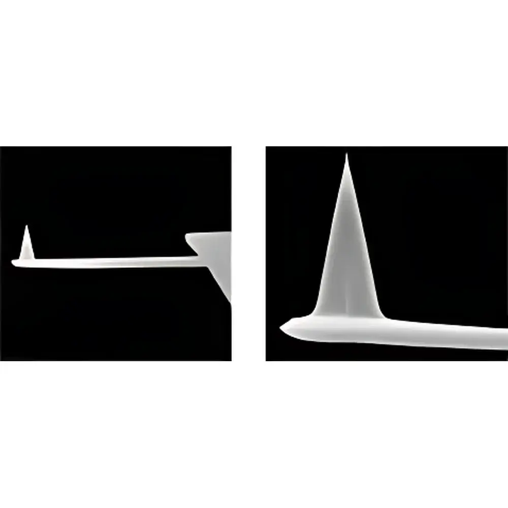
The Nanosensors NSG11/CSG11 series represents a benchmark in high-resolution silicon cantilever probes engineered for atomic force microscopy (AFM) in tapping (intermittent contact) mode. Designed for quantitative nanoscale topography and mechanical property mapping, these probes leverage precisely controlled silicon micromachining and electron-beam deposition to deliver exceptional tip sharpness, mechanical stability, and optical reflectivity. Each probe is fabricated from single-crystal silicon doped with boron at 5×10²⁰/cm³ — a concentration selected to suppress electrostatic charge accumulation during scanning of insulating or semi-conductive samples. The gold-coated backside enhances laser beam reflection efficiency by a factor of three compared to uncoated cantilevers, directly improving signal-to-noise ratio and feedback loop stability in commercial AFM systems. The NSG11/CSG11 platform supports both standard and ultra-sharp variants (S-series), where every tip undergoes post-fabrication SEM metrology to verify tip radius ≤10 nm — a critical specification for sub-10 nm lateral resolution in soft matter, 2D materials, and semiconductor surface characterization.
Key Features
- SEM-validated tip radius ≤10 nm (standard) or <5 nm (S-series on request), enabling high-fidelity imaging of atomic steps, graphene wrinkles, and polymer domain boundaries
- Double-cantilever chip architecture (two independent rectangular beams per substrate) for redundancy, method validation, and multi-parameter acquisition
- Au reflective coating applied via e-beam evaporation ensures uniform thickness, low stress, and long-term optical stability under repeated laser exposure
- Boron-doped silicon substrate provides intrinsic electrical conductivity while maintaining mechanical Q-factor >200 in air — essential for stable resonance tracking in amplitude-modulated AFM
- Compatible with all major AFM platforms including Bruker Dimension Icon, Keysight 5500/8500, Park NX-Series, NT-MDT Nova, and JPK NanoWizard systems
- GelPak® packaging (Vichem registered) minimizes mechanical damage and particulate contamination during handling and storage
Sample Compatibility & Compliance
NSG11/CSG11 probes are validated for use across diverse sample classes: conductive substrates (HOPG, Au(111), Si wafers), insulating oxides (SiO₂, Al₂O₃), biological membranes (supported lipid bilayers), polymeric thin films, and 2D materials (MoS₂, h-BN). Their chemical inertness and absence of catalytic residues ensure non-invasive imaging under ambient, liquid, or low-vacuum conditions. All probes comply with ISO/IEC 17025-accredited calibration practices for dimensional metrology; tip geometry verification follows ASTM E2539–21 guidelines for AFM probe certification. For regulated environments (e.g., pharmaceutical QC or microelectronics process control), traceable SEM calibration reports and lot-specific certificates of conformance are available upon request — supporting GLP/GMP documentation requirements and FDA 21 CFR Part 11 audit readiness.
Software & Data Management
While the NSG11/CSG11 is a passive hardware component, its performance is fully integrated into proprietary AFM software ecosystems. Bruker’s NanoScope Analysis v2.0+, Keysight’s PicoView, and Park Systems’ XEI support automated cantilever recognition, spring constant calibration (Sader method), and thermal tune-based resonance optimization. When paired with third-party analysis tools such as Gwyddion (open-source) or MountainsMap® (Digital Surf), users can perform tip deconvolution, roughness quantification (Sa, Sq, Sz per ISO 25178), and adhesion force mapping — all traceable to the certified tip geometry. Batch processing workflows accommodate large-scale probe qualification datasets, enabling statistical validation of tip wear and reproducibility across production lots.
Applications
- Nanomechanical mapping of modulus and adhesion on polymer blends and block copolymers
- Surface defect inspection of EUV photomasks and advanced node semiconductor wafers
- Topographic and phase contrast imaging of exfoliated transition metal dichalcogenides (TMDs)
- In-situ monitoring of protein adsorption kinetics on functionalized surfaces
- Quantitative roughness assessment of medical-grade titanium implants per ISO 10993-22
- Calibration artifact verification using NIST-traceable grating standards (e.g., PTB SRM 2051)
FAQ
What is the typical spring constant range for NSG11 probes?
The nominal spring constant is 5.5 ± 1.5 N/m, measured via static beam deflection and verified by thermal noise spectrum analysis. Custom calibration certificates report individual values per chip.
Can NSG11 be used in contact mode?
Yes, though optimized for tapping mode; contact-mode use requires careful load control (<1 nN) to prevent tip wear on hard substrates.
Is the gold coating compatible with electrochemical AFM (EC-AFM)?
Au-coated NSG11 is suitable for non-corrosive electrolytes (e.g., KCl, PBS); for aggressive media, TiN- or Pt-coated variants are recommended.
How should I store unused probes to maintain tip integrity?
Store in original GelPak® boxes inside desiccated, particle-free environments at 20–25°C; avoid UV exposure and repeated thermal cycling.
Do you provide batch-level metrology data?
Yes — SEM tip radius histograms, resonance frequency distributions, and reflectivity spectra are provided for each production lot upon request.


