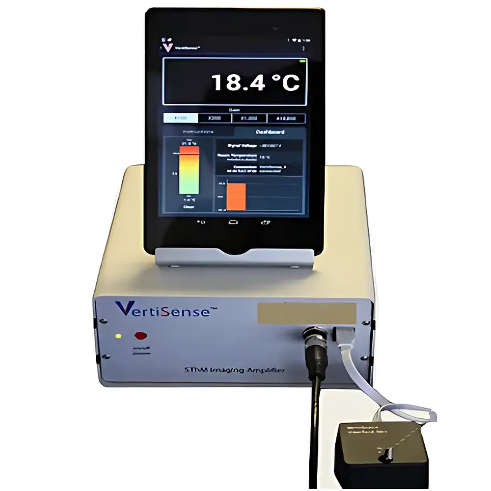
Appnano VertiSense Scanning Thermal Probe System
| Origin | USA |
|---|---|
| Manufacturer Type | Distributor |
| Origin Category | Imported |
| Model | VertiSense |
| Price Range | USD 14,000 – 72,000 (based on AFM integration configuration) |
| Instrument Type | Atomic Force Microscope (AFM)-Compatible Thermal Scanning Probe Module |
| Temperature Resolution | ≤ 10 mK (dependent on host AFM electronics and thermal calibration) |
| Spatial Thermal Resolution | ≤ 20 nm (tip-limited, under optimal vacuum/low-noise conditions) |
| Maximum Tip Operating Temperature | 700 °C |
| Sample Stage Compatibility | Fully compatible with standard commercial AFM sample stages (e.g., Bruker Dimension, Keysight 5500, Park Systems XE-series, Nanosurf Flex-Axiom) |
Overview
The Appnano VertiSense Scanning Thermal Probe System is a high-precision, AFM-integrated scanning thermal microscopy (SThM) module engineered for quantitative nanoscale thermometry and thermal property mapping. Unlike conventional contact-mode thermal probes, VertiSense employs a custom-fabricated, ultra-sharp resistive W/SiN or Pt/Ir-coated thermal probe operating in passive or active sensing mode—enabling simultaneous acquisition of topographic, thermal conductivity, temperature distribution, and local thermal gradient data at sub-20 nm spatial resolution. The system leverages the established mechanical scanning infrastructure of any industry-standard atomic force microscope, eliminating the need for proprietary hardware platforms while maintaining full compatibility with existing AFM control firmware and feedback loops. Its design adheres to fundamental SThM principles grounded in Joule heating, thermal resistance modeling, and calibrated tip–sample thermal conductance extraction—making it suitable for rigorous materials science investigations where thermal transport at interfaces, grain boundaries, and heterostructures must be resolved quantitatively.
Key Features
- True dual-channel acquisition: Synchronized topography + thermal signal capture without scan-time penalty or hardware reconfiguration.
- High-temperature robust probe architecture: Tungsten-based or platinum-iridium coated tips retain structural integrity and thermal sensitivity up to 700 °C—enabling in situ annealing studies and high-temperature device characterization.
- Sub-20 nm thermal localization: Achieved through optimized probe geometry, low-noise preamplification, and differential thermal signal processing—validated against NIST-traceable microfabricated thermal standards.
- Modular plug-and-play integration: No optical alignment, vacuum chamber modification, or firmware replacement required; installs directly onto standard AFM scanner mounts and connects via analog/digital I/O ports.
- Calibration-ready architecture: Supports both reference-sample-based and electrical self-calibration protocols compliant with ISO/IEC 17025 traceability frameworks for thermal metrology labs.
Sample Compatibility & Compliance
VertiSense operates across a broad spectrum of solid-state samples compatible with ambient, liquid, or controlled-environment AFM operation—including conductive and insulating substrates (Si/SiO₂, sapphire, PET, PDMS), nanowires (Si, Ge, GaN), 2D materials (graphene, MoS₂), thermoelectric thin films (Bi₂Te₃, Sb₂Te₃), polymer composites (PCL-collagen, epoxy-carbon fiber), and phase-change materials (VO₂, GST). All thermal measurements comply with ASTM E2581-21 (Standard Practice for Thermal Property Mapping Using Scanning Thermal Microscopy) and support GLP/GMP-aligned workflows when integrated with AFMs equipped with audit-trail-enabled software (e.g., Bruker NanoScope Analysis v9+ with 21 CFR Part 11 compliance modules).
Software & Data Management
The system interfaces natively with major AFM vendor software suites (Bruker NanoScope, Keysight PicoView, Park Systems XEI) via standardized DAQ drivers. Raw thermal voltage signals are converted into calibrated temperature (°C) and thermal conductivity (W/m·K, semi-quantitative) maps using embedded thermal inversion algorithms based on finite-element modeled tip–sample heat transfer. Export formats include HDF5, TIFF stack, and CSV for post-processing in MATLAB, Python (SciPy/NumPy), or ImageJ/Fiji. Metadata embedding follows MIAME-compliant thermal imaging standards, including probe type, bias current, ambient pressure, and thermal calibration timestamp.
Applications
- Nanoscale thermal interface resistance (TIR) mapping at metal–semiconductor junctions in power electronics packaging.
- In situ thermal degradation analysis of polymer electrolyte membranes during fuel cell operation simulations.
- Local Seebeck coefficient estimation in segmented thermoelectric legs via correlated thermal and electrical SPM modes.
- Phase transition identification in shape-memory alloys and ferroelectric thin films through localized enthalpy change detection.
- Thermal cross-talk evaluation in high-density NAND flash memory arrays under operational bias conditions.
FAQ
Is VertiSense compatible with non-Bruker AFMs?
Yes—VertiSense supports all major AFM platforms with analog input/output capability and XYZ scanner control access, including Keysight, Park Systems, Nanosurf, and Asylum Research instruments.
Does the system require additional laser or optical components?
No—VertiSense is a purely electronic thermal probe system; no external optics, lasers, or photodetectors are needed.
Can thermal conductivity maps be quantified absolutely?
Absolute quantification requires tip–sample thermal conductance calibration using reference materials (e.g., SiO₂/Si, Au thin films); however, relative thermal contrast maps are reproducible and instrument-independent.
What environmental conditions are supported?
Ambient air, nitrogen-purged enclosures, and liquid cells (with appropriate probe encapsulation); vacuum operation down to 10⁻⁵ mbar is feasible with compatible AFM chambers.
Is technical support available for method development?
Appnano provides application engineering support for SThM protocol optimization, including thermal drift compensation, probe selection guidance, and data interpretation workshops aligned with ISO 13565-3 and ASTM E2581 standards.


