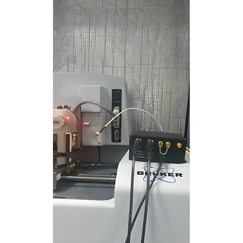
PrimeNano sMIM Microwave Scanning Impedance Microscope
| Origin | USA |
|---|---|
| Manufacturer Type | Authorized Distributor |
| Origin Category | Imported |
| Model | Prime |
| Price Range | USD 135,000 – 205,000 |
| Instrument Type | Atomic Force Microscope (AFM)-Based Scanning Microwave Impedance Microscope |
| Positional Detection Noise | 0.01 nm |
| Scan Area | 20 µm × 20 µm (model-dependent) |
| Stage Travel Range | 100 µm × 100 µm × 10 µm |
Overview
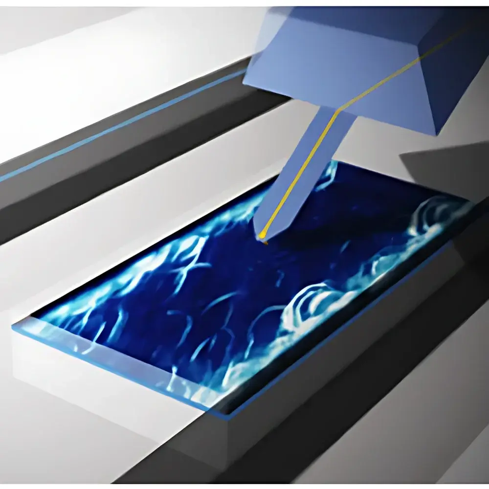
The PrimeNano sMIM Microwave Scanning Impedance Microscope is an AFM-integrated near-field microwave probe system engineered for quantitative nanoscale electrical characterization. Operating on the principle of scanning microwave impedance microscopy (sMIM), it couples a high-frequency (typically 1–20 GHz) microwave signal with dynamic AFM feedback to resolve local variations in complex impedance—specifically capacitance (C), conductance (G), and their voltage derivatives (dC/dV, dG/dV)—with sub-50 nm spatial resolution. Unlike conventional electrical AFM modes (e.g., KPFM or C-AFM), sMIM enables non-contact, non-destructive subsurface probing beyond 100 nm depth in dielectrics and semiconductors, making it uniquely suited for carrier profiling, dopant mapping, ferroelectric domain analysis, and buried interface inspection in multilayer thin-film devices.
Key Features
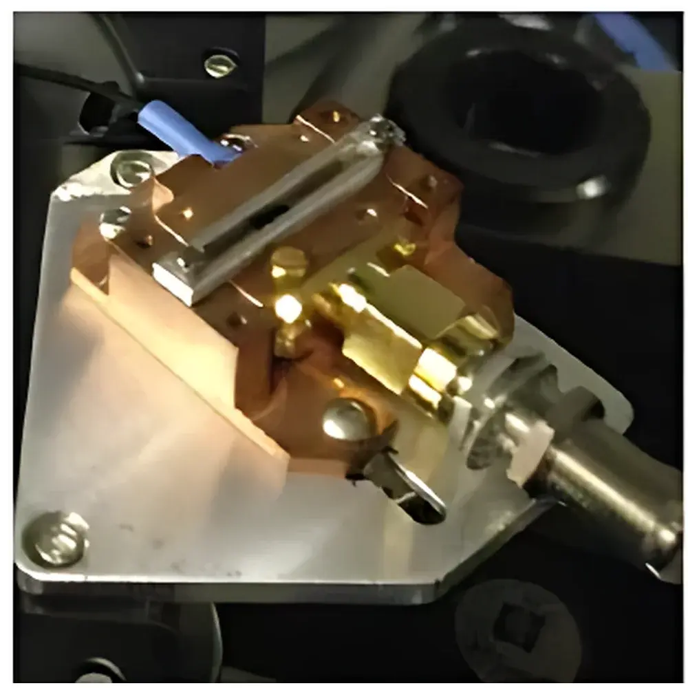
- Sub-50 nm lateral resolution in both topographic and electrical imaging channels, enabled by proprietary coaxially shielded MEMS-based sMIM probes that suppress stray electromagnetic coupling and parasitic radiation.
- Simultaneous acquisition of multiple electrical contrast mechanisms within a single scan: sMIM-C (capacitance & εr), sMIM-R (conductance & σ), dC/dV amplitude (carrier concentration), dC/dV phase (carrier type: electrons vs. holes), dR/dV amplitude/phase (dielectric loss & charge trapping dynamics).
- Low-noise positional detection (<0.01 nm RMS) ensures high-fidelity correlation between topography and nanoscale electrical heterogeneity—even on rough or insulating surfaces.
- Modular sMIM scan head compatible with major commercial AFM platforms (e.g., Bruker Dimension, Park NX, Oxford Instruments Cypher), requiring no modification to host instrumentation.
- Integrated microwave source, interferometric signal conditioning unit, and real-time lock-in demodulation architecture optimized for stability under ambient and controlled-environment conditions.
- Full compatibility with contact, tapping, and force-curve modes—electrical data acquisition remains active during mechanical spectroscopy, enabling correlative nanomechanical–electrical property mapping.
Sample Compatibility & Compliance
The sMIM system accommodates diverse material classes without conductive coating or vacuum requirements: conductors (metals, graphene), semiconductors (Si, GaN, MoS2, perovskites), wide-bandgap insulators (Al2O3, HfO2), ferroelectrics (PZT, BTO), and soft functional polymers. Its non-invasive nature supports ISO/IEC 17025-aligned metrology workflows and complies with ASTM E2948 (Standard Guide for Electrical Characterization of Nanomaterials) and IEC 62607-5-3 (Nanomanufacturing—Material Specifications—Part 5-3: Graphene—Electrical Properties). All firmware and software modules support audit-trail logging and user-access controls consistent with GLP/GMP documentation standards.
Software & Data Management
ScanWave™ software provides a unified interface for instrument control, real-time signal processing, and multi-parameter image reconstruction. It includes automated calibration routines for microwave tip-sample impedance matching, drift-compensated time-lapse electrical imaging, and batch-processing pipelines compliant with FAIR (Findable, Accessible, Interoperable, Reusable) data principles. Export formats include HDF5 (with embedded metadata per NIEM/ISO 11179), TIFF (32-bit float), and CSV for third-party analysis (e.g., MATLAB, Python SciPy, Gwyddion). The software architecture conforms to FDA 21 CFR Part 11 requirements for electronic records and signatures when deployed in regulated R&D environments.
Applications
- Nanoscale dopant profiling and junction depth validation in advanced CMOS and FinFET test structures.
- Domain wall dynamics and polarization switching behavior in ferroelectric thin films and heterostructures.
- Interface trap density quantification at semiconductor/dielectric interfaces (e.g., Si/SiO2, GaN/AlGaN).
- Carrier mobility and scattering mechanism analysis in 2D materials (graphene, TMDs) and van der Waals heterostructures.
- Defect-assisted leakage path identification in high-κ gate stacks and memristive oxide layers.
- Non-destructive evaluation of embedded interconnect integrity and void formation in advanced packaging substrates.
FAQ
What AFM platforms are compatible with the PrimeNano sMIM module?
The sMIM scan head integrates mechanically and electronically with Bruker Dimension Icon/Edge, Park Systems NX series, and Oxford Instruments Cypher ES systems via standardized mounting interfaces and API-level communication protocols.
Can sMIM perform subsurface imaging through insulating layers?
Yes—microwave near-fields penetrate dielectrics up to ~150 nm deep depending on frequency, permittivity, and loss tangent; depth sensitivity is tunable via carrier frequency selection and lock-in phase analysis.
Is vacuum or cryogenic operation supported?
The base sMIM configuration operates under ambient conditions; optional environmental chambers (temperature-controlled, inert gas, or low-vacuum) are available for specialized applications requiring thermal or atmospheric stabilization.
How is electrical calibration performed?
Calibration uses certified reference samples (e.g., doped Si wafers with known carrier concentrations, parallel-plate capacitors with traceable εr) and is traceable to NIST SRM standards via documented uncertainty budgets.
Does the system support automated batch scanning for process monitoring?
Yes—ScanWave™ includes scriptable macro functionality and integration with SECS/GEM protocols for unattended multi-site scanning across wafers or sample arrays, suitable for inline QC in pilot-line environments.


