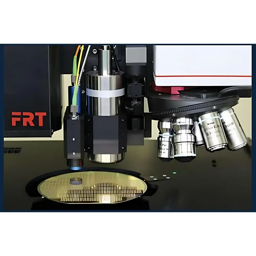
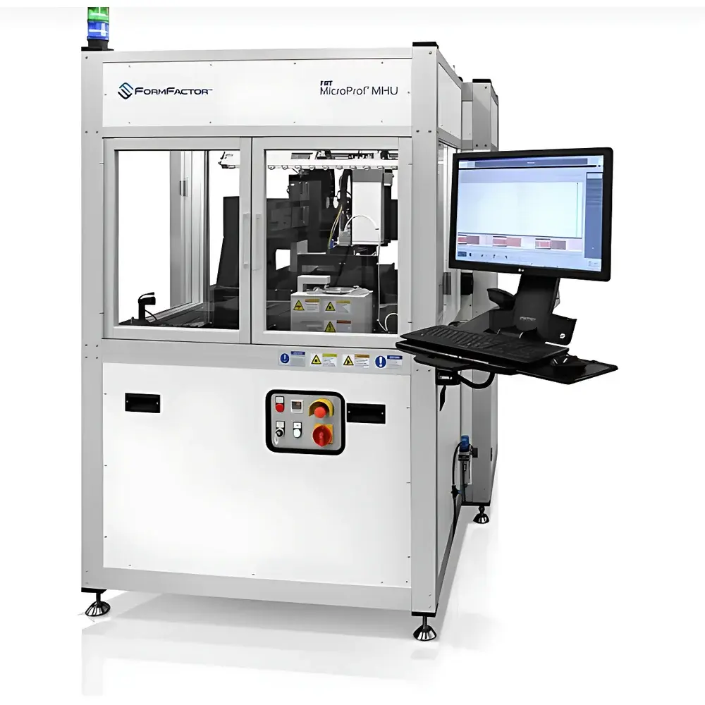
TTV Surface Profilometry System – FRT MicroProf MHU
| Brand | FRT |
|---|---|
| Origin | Germany |
| Model | MicroProf MHU |
| Wafer Handling | Semi-Automatic with Material Handling Unit (MHU) |
| Throughput | Up to 220 wafers/hour |
| Wafer Diameter Support | 2″ to 8″ |
| Cassette Capacity | Up to 4 open FOUPs/SMIF pods |
| Integrated Options | Pre-aligner, OCR reader |
| Application Focus | Semiconductor, MEMS, Sapphire, LED wafer manufacturing |
Overview
The FRT MicroProf MHU is a semi-automated surface profilometry system engineered for high-precision total thickness variation (TTV), bow, warp, and surface topography measurement of bare, coated, and patterned wafers in advanced microfabrication environments. Utilizing non-contact optical interferometry—specifically phase-shifting white-light interferometry (PSI/WLI)—the system delivers sub-nanometer vertical resolution and nanometer-level repeatability across full-wafer scans. Its integrated Material Handling Unit (MHU) enables unattended operation in cleanroom-compatible workflows, making it suitable for inline or offline metrology stations in semiconductor front-end processes, MEMS device fabrication, sapphire substrate evaluation, and LED epitaxial layer development. The system operates under ISO 14644-1 Class 5 cleanroom conditions and complies with SEMI S2/S8 safety and ergonomics standards.
Key Features
- Semi-automated wafer handling via dual-vacuum end-effectors on a high-speed robotic arm, achieving up to 220 wafers per hour with minimal operator intervention
- Full-wafer scanning capability for diameters from 50 mm (2″) to 200 mm (8″), supporting both standard and custom wafer formats
- Modular cassette station accommodating up to four open FOUPs or SMIF pods, configurable for front-opening or side-loading integration
- Optional pre-aligner module for edge-based wafer centering and orientation correction prior to measurement
- Integrated OCR reader for automated wafer identification and traceability, compatible with industry-standard barcode and DataMatrix symbologies
- Rugged mechanical architecture with vibration-damped granite base and active temperature stabilization (±0.1 °C) to ensure long-term measurement stability
- Compliance-ready design supporting audit trails, electronic signatures, and user access control per FDA 21 CFR Part 11 requirements when paired with FRT’s certified software suite
Sample Compatibility & Compliance
The MicroProf MHU is validated for use with silicon, sapphire, SiC, GaN, glass, and quartz wafers—both unpatterned and post-lithography. It supports measurement of photoresist films, dielectric stacks (e.g., SiO₂, Si₃N₄), metal layers (Al, Cu, Ti), and MEMS-relevant thin-film structures without risk of surface damage. All measurement protocols adhere to ASTM F397 (Standard Test Method for Total Thickness Variation of Silicon Wafers) and ISO 14407 (Semiconductor devices — Mechanical and physical tests — Measurement of wafer thickness and thickness variation). System qualification documentation—including IQ/OQ/PQ templates—is provided to support GLP and GMP-regulated environments.
Software & Data Management
Controlled by FRT’s proprietary Profilometer Software Suite (v8.x), the system provides real-time visualization of TTV maps, cross-sectional line profiles, and statistical process control (SPC) dashboards. Raw interferometric data is stored in vendor-neutral HDF5 format with embedded metadata (timestamp, operator ID, recipe name, environmental logs). The software supports automated report generation compliant with ISO/IEC 17025 requirements, including uncertainty budgeting per GUM (Guide to the Expression of Uncertainty in Measurement). Data export interfaces include OPC UA, SECS/GEM, and SQL database connectors for MES and factory automation integration.
Applications
- Post-CMP TTV verification of silicon wafers prior to epitaxial growth or device processing
- Thickness uniformity assessment of sapphire substrates used in GaN-on-sapphire LED manufacturing
- Bow and warp characterization of MEMS wafers after bonding, annealing, or deep reactive ion etching (DRIE)
- Photoresist film thickness and develop uniformity monitoring across lithography tool qualification cycles
- Quality gate inspection for compound semiconductor foundries producing RF and power devices
- Process window validation during thin-film deposition (PVD, CVD, ALD) and etch tool matching studies
FAQ
What wafer sizes does the MicroProf MHU support?
The system handles wafers from 2″ (50 mm) to 8″ (200 mm) in diameter, with configurable chuck adapters for non-standard geometries.
Is the system compatible with 300 mm wafer fabs?
No—the MHU variant is optimized for ≤200 mm wafers; FRT offers the MicroProf 300 platform for 300 mm applications.
Can TTV measurements be performed on patterned wafers with high aspect-ratio features?
Yes—phase-shifting interferometry enables robust height reconstruction even on structured surfaces with feature heights up to 10 µm and lateral pitches down to 2 µm.
Does the system require external vibration isolation?
The granite base and internal damping are sufficient for typical Class 5 cleanroom floors; no active isolation table is required unless ambient vibration exceeds 25 µm/s RMS.
How is measurement traceability maintained?
Each system ships with NIST-traceable calibration artifacts and a full calibration certificate; annual recalibration services are available through FRT’s DAkkS-accredited service centers in Europe and Asia.


