Nanofabrication Custom Grating Service (Extreme-Scale & Specialty-Function Diffraction Gratings)
| Origin | Jiangsu, China |
|---|---|
| Manufacturer Type | Authorized Distributor |
| Regional Origin | Domestic (PRC) |
| Model | Custom Grating Fabrication |
| Pricing | Available Upon Technical Consultation |
Overview
This nanofabrication service delivers custom-engineered diffraction gratings optimized for extreme-scale optical metrology, high-resolution spectroscopy, and precision motion feedback systems. Leveraging a hybrid process flow—integrating nanoimprint lithography (NIL), electron-beam evaporation, and reactive ion etching (RIE)—the service achieves sub-100 nm grating periods with high aspect ratio, low sidewall roughness, and exceptional period uniformity across wafer-scale substrates. The core measurement principle relies on first-order Bragg diffraction under monochromatic or broadband illumination, where groove density, profile fidelity (blaze angle, duty cycle), and material refractive index directly determine diffraction efficiency, polarization response, and spectral dispersion characteristics. Designed for integration into interferometric encoders, space-borne spectrometers, and inertial navigation reference systems, these gratings operate in transmission or reflection modes, supporting both UV–VIS and near-IR spectral bands (193–1550 nm).
Key Features
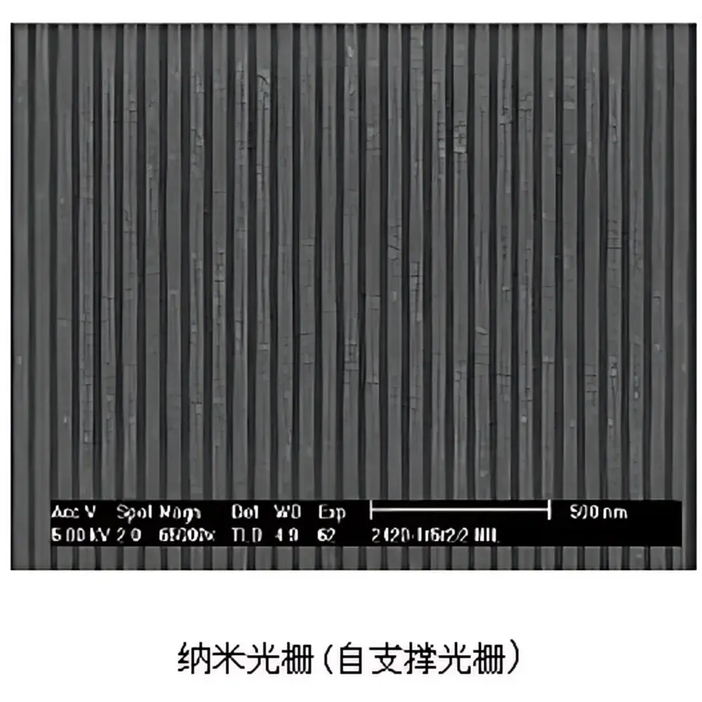
- Sub-100 nm minimum grating period (down to 80 nm demonstrated), corresponding to line densities up to 12,500 lines/mm
- High-fidelity trapezoidal or blazed groove profiles fabricated via RIE with <±2 nm critical dimension (CD) uniformity over 50 mm × 50 mm areas
- Material flexibility: Si, fused silica, CaF₂, sapphire, and silicon nitride substrates; Cr, Au, Al, Ni, and Ti-based reflective/transmissive coatings deposited by e-beam evaporation
- Self-supporting free-standing metal transmission gratings with mechanical stability >10⁶ cycles under 1 g acceleration (validated per MIL-STD-810H, Method 514.7)
- Process traceability: Each batch includes SEM cross-section imaging, AFM roughness mapping (Rq < 0.8 nm), and diffraction efficiency calibration at λ = 632.8 nm and λ = 1550 nm
Sample Compatibility & Compliance
The service accommodates customer-supplied wafers (Ø50–150 mm, thickness 0.3–1.0 mm) or provides standard substrates with optional AR/HR coatings. All fabrication steps comply with cleanroom Class 100 (ISO 5) protocols. Final products meet ISO 10110-7 (surface imperfections) and ISO 14644-1 (particulate cleanliness). For defense-related applications, documentation supports ITAR-controlled export classification (ECCN 3A001.b.2.a) and includes full process audit trails suitable for DoD DD Form 250 submission. In civil nuclear instrumentation contexts, grating assemblies are compatible with ASME NQA-1–2022 requirements when integrated into certified detector modules.
Software & Data Management
No embedded firmware or proprietary control software is provided—gratings are passive optical components. However, comprehensive metrology datasets (SEM image stacks, AFM height maps, Littrow-angle efficiency curves, and CD distribution histograms) are delivered in vendor-neutral formats: TIFF (images), CSV (numerical data), and PDF (certification reports). All files adhere to the FAIR principles (Findable, Accessible, Interoperable, Reusable) and include embedded XMP metadata referencing ASTM E2918–22 (standard guide for reporting nanoscale characterization data). Traceable calibration certificates conform to ISO/IEC 17025:2017 and support GLP-compliant lab audits.
Applications
- Ultra-high-resolution Czerny–Turner and echelle spectrometers for plasma diagnostics (fusion research) and exoplanet atmospheric analysis
- Interferometric linear and rotary encoders in semiconductor stepper stages and EUV lithography alignment systems
- Polarization-sensitive grating couplers for silicon photonics I/O interfaces operating at 1310/1550 nm
- Compact Fourier-transform infrared (FTIR) spectrometer cores used in airborne radiometric monitoring of nuclear fission signatures
- Inertial measurement units (IMUs) employing laser Doppler vibrometry with phase-encoded grating references for missile guidance terminal homing
FAQ
What is the minimum order quantity (MOQ) for custom grating fabrication?
The MOQ is one process run per mask design, typically accommodating up to four 50-mm wafers or two 100-mm wafers per batch. Smaller proof-of-concept samples (10 mm × 10 mm chips) are available under NDA.
Do you support DOE (diffractive optical element) or chirped grating designs?
Yes—custom phase profiles, including linearly chirped, quadratic, and quasi-periodic structures, are supported using vector-scan e-beam writing prior to NIL master stamp fabrication.
Can gratings be qualified for spaceflight environments?
Gratings have undergone thermal vacuum cycling (–40 °C to +85 °C, 10 cycles), proton irradiation (10¹⁰ p/cm², 60 MeV), and random vibration testing (14.1 g rms, 20–2000 Hz); qualification reports available upon request.
Is process IP transfer or joint development possible?
Yes—technology transfer packages—including process recipes, mask layout guidelines, and failure mode analysis (FMEA) documentation—are available under bilateral IP agreements aligned with IEEE Std 1471–2000 and ISO/IEC 29119–3.
How is dimensional stability verified over time?
Accelerated aging tests per ASTM E1541–21 (optical component lifetime prediction) confirm <0.1% period drift after 10,000 hours at 60 °C and 85% RH, measured via laser interferometric autocollimation.


