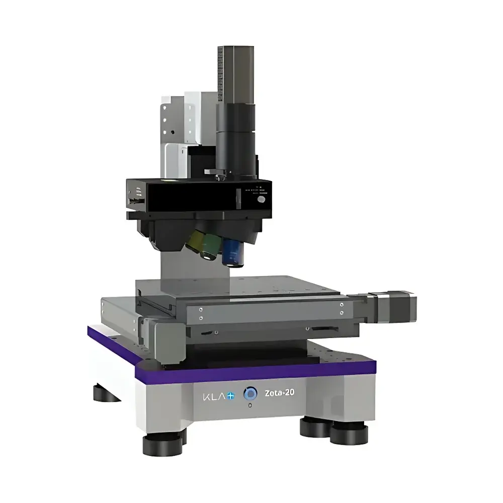
KLA Zeta-20 Desktop Optical Profilometer
| Brand | KLA |
|---|---|
| Origin | USA |
| Model | Zeta-20 |
| Product Type | Non-contact 3D Optical Profilometer / Surface Roughness Analyzer |
| Measurement Principles | ZDot™ Multi-Mode Imaging, White Light Interferometry (WLI), Nomarski Differential Interference Contrast (DIC), Shear Interference, Broadband Reflectometry, Automated Optical Inspection (AOI) |
| Vertical Resolution | Sub-nanometer (typical, dependent on mode) |
| Lateral Resolution | ~0.4 µm (optical diffraction-limited) |
| Step Height Range | 1 nm – 10 mm |
| Surface Roughness Range | Ra 0.01 nm – 50 µm |
| Film Thickness Range | 30 nm – 100 µm (transparent films) |
| Defect Detection Limit | ≥1 µm |
| Field of View | Up to 8 mm × 6 mm (configurable via objective lenses) |
| Objective Lenses | 2.5×, 5×, 10×, 20×, 50×, 100× (motorized turret) |
| Software Platform | ZetaWare™ v6.x (GLP/GMP-compliant, 21 CFR Part 11 ready) |
Overview
The KLA Zeta-20 Desktop Optical Profilometer is a high-precision, non-contact 3D surface metrology system engineered for comprehensive topographic characterization in R&D and high-mix manufacturing environments. Leveraging KLA’s proprietary ZDot™ multi-modal optical architecture, the Zeta-20 integrates six complementary measurement technologies—ZDot™ imaging, white light interferometry (ZXI), Nomarski interference contrast (ZIC), shear interference (ZSI), integrated broadband reflectometry (ZFT), and automated optical inspection (AOI)—within a single compact benchtop platform. Unlike conventional profilometers constrained by sample reflectivity or transparency, the Zeta-20 delivers robust, quantitative 3D data across heterogeneous surfaces: from highly reflective silicon wafers and low-reflectance polymer films to transparent multilayers, rough MEMS structures, and patterned photovoltaic textures. Its core strength lies in simultaneous acquisition of nanoscale vertical resolution and true-color, extended-depth-of-field imaging—enabling correlation between surface geometry, optical appearance, and process-induced features without physical contact or vacuum requirements.
Key Features
- ZDot™ Technology: Captures high-fidelity 3D topography and True Color infinite-focus images in a single scan—eliminating focus stacking artifacts and preserving spatial registration between morphology and visual context.
- Multi-Mode Optical Engine: Selects optimal measurement physics per region-of-interest—WLI for high-z-resolution broad-area mapping, ZIC for sub-nanometer roughness quantification on smooth dielectrics, ZSI for vibration-insensitive high-slope profiling, and ZFT for non-destructive film thickness and refractive index extraction.
- Motorized Objective Turret: Supports six magnifications (2.5×–100×) with auto-calibrated calibration traceability; enables seamless transition from macro-scale warpage analysis to sub-micron defect morphology assessment.
- Integrated AOI & KLARF Navigation: Performs automated defect detection ≥1 µm, then navigates directly to defect coordinates using industry-standard KLARF files for localized 3D reconstruction—critical for failure analysis in semiconductor packaging and advanced PCB lines.
- ZetaWare™ Software Suite: Includes ASTM E2799-compliant roughness parameter calculation (Ra, Rq, Rz, Sa, Sq), ISO 25178 texture analysis (Spk, Sk, Svk), stress-induced curvature modeling (Stoney equation integration), and configurable SOP-driven workflows with full audit trail and electronic signature support.
Sample Compatibility & Compliance
The Zeta-20 accommodates samples up to 200 mm × 200 mm × 50 mm (custom stages available), including bare wafers, diced dies, flexible substrates, medical microfluidic chips, and textured solar cell surfaces. It requires no conductive coating, vacuum, or destructive preparation—making it suitable for soft polymers, biological coatings, and delicate nanostructured surfaces. The system complies with ISO/IEC 17025 calibration traceability standards, supports GLP/GMP documentation requirements, and its software architecture meets FDA 21 CFR Part 11 criteria for electronic records and signatures when configured with role-based access control and immutable audit logs.
Software & Data Management
ZetaWare™ v6.x provides a unified interface for instrument control, real-time visualization, batch processing, and report generation. All raw interferograms, ZDot™ stacks, reflectance spectra, and AOI maps are stored in vendor-neutral HDF5 format with embedded metadata (timestamp, operator ID, calibration ID, environmental conditions). Scriptable automation via Python API enables integration into factory MES systems and statistical process control (SPC) dashboards. Measurement recipes—including stage motion paths, focus search parameters, and analysis masks—can be version-controlled and deployed across multiple instruments for cross-site method equivalence.
Applications
- Step height metrology for lithography validation, etch depth monitoring, and CMP endpoint control—from atomic-layer-deposited films (1 nm steps) to wafer-level encapsulation bumps (5 mm height).
- Surface texture analysis per ISO 25178 and ASME B46.1: quantifying functional parameters (Sk, Spk, Svk) for tribological performance prediction in MEMS actuators and implantable device surfaces.
- Thin-film metrology on patterned substrates: measuring thickness uniformity and optical constants of anti-reflective, passivation, and barrier layers without masking or reference standards.
- Warpage and翘曲 (3D shape) analysis of fan-out WLP panels and flexible PCBs using stitched large-area topography and best-fit plane deviation mapping.
- Defect root-cause analysis: correlating AOI-detected particles, scratches, or delamination with their 3D morphological signature—depth, volume, edge slope—to distinguish process-related vs. handling-induced anomalies.
FAQ
What vertical resolution can the Zeta-20 achieve in different modes?
Sub-nanometer vertical repeatability is typical in ZIC mode on smooth SiO₂; WLI achieves <0.1 nm phase noise floor under controlled lab conditions; ZDot™ delivers ~0.5 nm effective resolution depending on surface slope and coherence.
Does the system require external vibration isolation?
No active isolation table is required for standard operation; the Zeta-20 incorporates passive damping and real-time fringe stabilization algorithms—validated for use on standard optical tables in Class 1000 cleanrooms.
Can Zeta-20 measure transparent films on transparent substrates?
Yes—using ZFT broadband reflectometry with multi-layer optical modeling (e.g., SiO₂ on fused silica, ITO on glass); accuracy depends on known dispersion models and substrate homogeneity.
Is GLP/GMP compliance supported out-of-the-box?
ZetaWare™ includes configurable audit trail, user authentication, electronic signatures, and SOP locking—but formal validation (IQ/OQ/PQ) must be performed by the end user per internal quality procedures.
How is calibration maintained across multiple instruments in a fab?
KLA provides NIST-traceable step height and roughness calibration standards; ZetaWare™ supports inter-instrument bias correction via reference sample trending and automated calibration verification protocols.