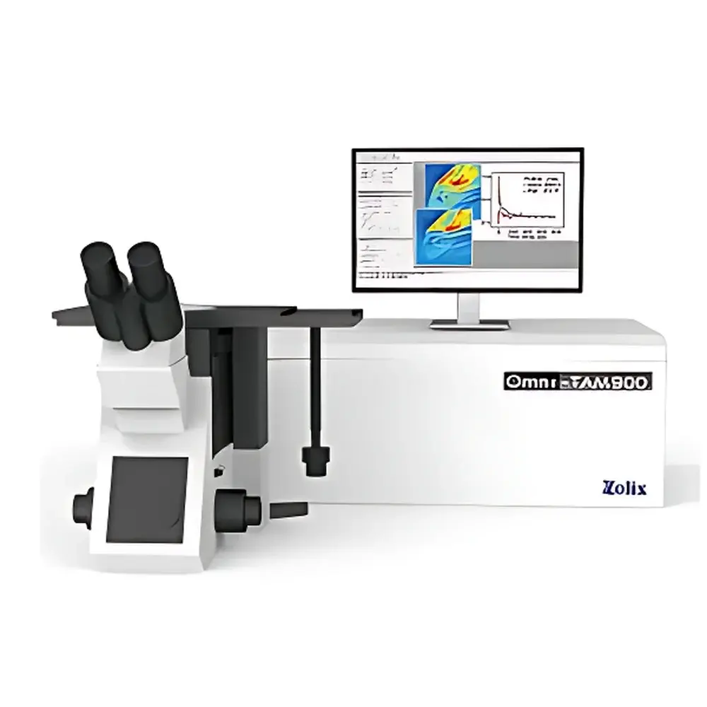
ZOLIX Omni-TAM900 Wide-Field Femtosecond Transient Absorption Imaging System
| Brand | ZOLIX |
|---|---|
| Origin | Beijing, China |
| Model | Omni-TAM900 Wide-Field Femtosecond Transient Absorption Imaging System |
| Detector | sCMOS camera |
| Spatial Resolution | 500 nm |
| Carrier Localization Accuracy | 30 nm |
| Temporal Resolution | 500 fs (with 100-fs laser pulses) |
| Optical Delay Range | 0–4 ns / 0–8 ns |
| Microscope Configuration | Inverted microscope with open-top design for cryostat, probe station, electrical gating, and magnetic field integration |
| Operating Modes | Point Pump / Wide-Field Probe |
| Sample Illumination Geometry | Reflectance or scattering |
Overview
The ZOLIX Omni-TAM900 Wide-Field Femtosecond Transient Absorption Imaging System is an integrated ultrafast optical platform engineered for spatiotemporal mapping of photogenerated carriers, excitons, and energy transfer dynamics at nanoscale spatial and femtosecond temporal resolutions. Based on the pump-probe principle, the system employs collinear or non-collinear femtosecond excitation and broadband probe pulses to quantify differential absorption (ΔA) across a two-dimensional field of view—enabling direct visualization of carrier migration, thermal diffusion, exciton localization, and heterogeneous physical state distribution in functional materials. Unlike point-scanning transient absorption microscopes, the Omni-TAM900 implements wide-field detection architecture coupled with interferometric signal amplification—a proprietary technique developed by ZOLIX—to enhance signal-to-noise ratio (SNR) without compromising acquisition speed. This architecture supports quantitative imaging at single-particle sensitivity, including monolayer graphene, sub-10-nm metallic nanoparticles, and molecular monocrystals.
Key Features
- Two operational configurations: (1) focused pump beam with wide-field probe illumination for carrier drift/diffusion velocity mapping; (2) wide-field pump + wide-field probe for spatially resolved carrier density, lifetime, and heterogeneity analysis
- Sub-500 nm diffraction-limited spatial resolution enabled by high-NA inverted microscope optics and optimized sCMOS sensor pixel binning
- 30 nm carrier localization precision achieved via centroid fitting of ΔA contrast profiles under stabilized mechanical and thermal conditions
- 500 fs effective time resolution, compatible with 100-fs Ti:sapphire or Yb-based oscillator-amplifier systems and optical parametric amplifiers (OPA)
- Open-top inverted microscope design accommodates in situ integration of cryogenic stages (4 K–300 K), electrical biasing probes, vector magnet systems (±9 T), and environmental control chambers
- Interferometric amplification module improves weak ΔA signals (down to 10−5 ΔOD) while suppressing common-mode laser intensity noise
Sample Compatibility & Compliance
The Omni-TAM900 is designed for solid-state thin films, 2D heterostructures, perovskite polycrystals, plasmonic nanostructures, and biological photosynthetic complexes mounted on standard glass or quartz substrates. It supports reflectance and scattering geometries—critical for opaque, highly scattering, or substrate-integrated samples where transmission is inaccessible. The system complies with ISO/IEC 17025 guidelines for measurement uncertainty estimation in ultrafast spectroscopy, and its delay-stage calibration traceability follows NIST-referenced interferometric standards. All optical components meet RoHS Directive 2011/65/EU requirements. Data acquisition workflows are structured to support GLP-compliant documentation, including timestamped metadata logging (laser energy, stage position, ambient temperature/humidity) and audit-ready file naming conventions aligned with FAIR data principles.
Software & Data Management
The proprietary ZOLIX TA-Imager software provides synchronized control of optical delay line, laser repetition rate, sCMOS exposure timing, and motorized filter wheels. It enables real-time background subtraction, flat-field correction, and pixel-wise kinetic decay fitting using multi-exponential or stretched exponential models. Export formats include HDF5 (with embedded metadata), TIFF stacks, and CSV-compatible kinetics tables. Time-resolved image sequences are automatically registered to reference frames using sub-pixel cross-correlation algorithms to correct for sample drift during long acquisitions. Software modules support batch processing of >1000 delay points per dataset and integrate with Python-based analysis environments (e.g., SciPy, NumPy, scikit-image) via documented APIs. All user actions—including parameter changes, ROI selections, and fit constraints—are logged with timestamps and operator IDs, satisfying FDA 21 CFR Part 11 requirements for electronic records and signatures when configured with optional audit-trail licensing.
Applications
The Omni-TAM900 addresses core challenges in ultrafast materials science, including carrier transport anisotropy in twisted 2D heterostructures (e.g., MoS2/WSe2), hot-carrier extraction efficiency at perovskite/metal oxide interfaces, phonon-mediated thermal diffusion in cubic boron arsenide, and edge-state exciton dynamics in WS2 monolayers. Published studies using this platform have quantified lateral carrier mobility in CsPbBr3 nanowires (J. Am. Chem. Soc. 2022, 144, 13928), mapped nanoscale “hot spots” in plasmon-enhanced photocatalysts, and resolved picosecond-scale charge separation gradients across grain boundaries in polycrystalline organic photovoltaics. Its capability to operate under cryogenic, high-magnetic-field, or electrochemical conditions extends utility into correlated electron systems such as cuprate superconductors and topological insulators.
FAQ
What laser sources are compatible with the Omni-TAM900?
The system is optimized for Ti:sapphire oscillators (700–1000 nm) and OPAs (240–2600 nm), but supports Yb-based amplifiers (1030 nm fundamental, tunable IR/UV via harmonic generation). Custom OPA integration services are available.
Can the system perform polarization-resolved transient absorption imaging?
Yes—motorized rotating waveplates and polarizers can be added to both pump and probe arms for full Stokes parameter acquisition and anisotropy mapping.
Is vacuum or inert-gas sample environment supported?
The open-top microscope stage allows integration of glovebox-compatible sample holders and differential pumping stages for air-sensitive 2D materials.
How is calibration performed for spatial and temporal axes?
Spatial calibration uses NIST-traceable USAF 1951 target imaging; temporal calibration employs autocorrelation of residual pump-probe overlap and known material response functions (e.g., GaAs exciton decay).
Does the system support third-party data analysis tools?
Yes—HDF5 output includes standardized metadata groups (NXentry, NXdata) compliant with NeXus format, enabling native import into Igor Pro, MATLAB, and open-source tools like silx or PyMca.


