CEL-SPS1000 Surface Photovoltage Spectrometer (SPV/SPC/SPS)
| Brand | CEL (China Education Goldsource) |
|---|---|
| Origin | Beijing, China |
| Manufacturer Type | OEM Manufacturer |
| Product Origin | Domestic (China) |
| Model | CEL-SPS1000 Surface Photovoltage Spectrometer (SPV/SPC/SPS) |
| Light Source Type | Multi-lamp Modular Source System (Xenon, Halogen, Deuterium) |
| Illumination Mode | External Irradiation Configuration |
| Voltage Detection Limit | >100 nV |
| Current Detection Limit | >100 pA |
| Phase Detection Range | –180° to +180° |
| Spectral Range | 200–1600 nm |
| Spectral Resolution | 0.1 nm |
| Wavelength Accuracy | ±0.1 nm |
| Monochromator Focal Length | 300 mm |
| Optical Design | Asymmetric Horizontal Czerny–Turner |
| Grating Size | 55 × 55 mm |
| Minimum Step Size | 0.0023 nm |
| Chopper Frequency Range | 20 Hz–10 kHz |
| Lock-in Amplifier Bandwidth | 1 mHz–102.4 kHz |
| Phase Resolution | 0.01° |
| Time Constant Range | 10 µs–30 ks |
| Filter Wheel | 6-position Automated, Standard Filters: 185–1600 nm |
| Light Source Power Control | 250–500 W (Xe lamp, software-regulated via USB) |
Overview
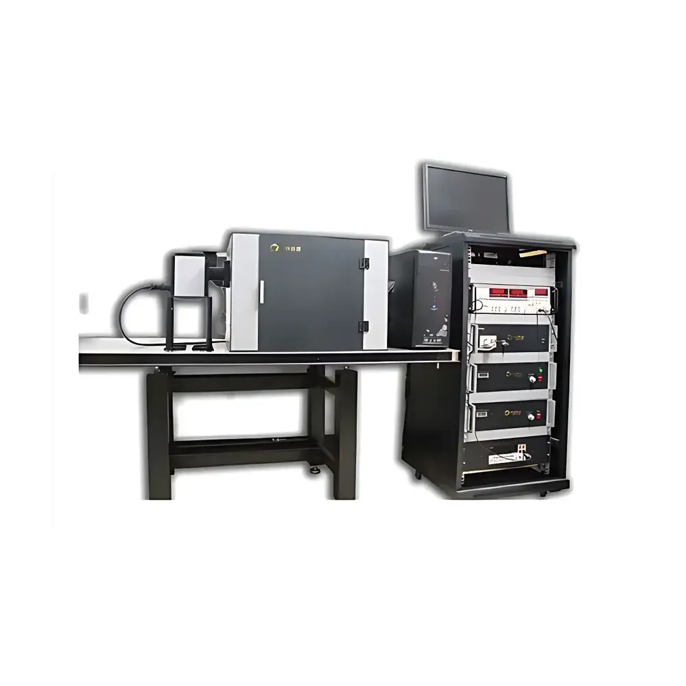
The CEL-SPS1000 Surface Photovoltage Spectrometer is a fully integrated, research-grade optical instrumentation platform engineered for quantitative analysis of surface photovoltage (SPV), surface photocurrent (SPC), and phase-resolved photovoltage spectroscopy (SPS). Based on the principle of modulated photon-induced surface charge displacement in semiconductors, the system detects minute changes in surface potential or current—typically within the top 10–50 nm of a material—under monochromatic illumination. This non-contact, non-destructive technique relies on lock-in detection to extract weak photoresponse signals from thermal and electronic noise, enabling high-fidelity spectral mapping of surface states, band alignment, carrier diffusion length, and interfacial charge separation dynamics. Unlike bulk-sensitive techniques such as conventional UV-Vis absorption or photoluminescence, SPV spectroscopy provides direct insight into surface/interface electronic structure without interference from substrate contributions—making it indispensable for evaluating heterojunctions, quantum dot assemblies, perovskite interfaces, and photoelectrode architectures used in solar fuel generation and photodetector development.
Key Features
- Fully automated, closed-path optical architecture housed in a light-tight dark chamber to eliminate ambient stray light and ensure signal integrity.
- Triple-lamp modular light source system: 500 W xenon lamp (200–1100 nm), halogen lamp (400–1600 nm), and deuterium lamp (190–400 nm), each with software-controlled intensity regulation and beam focusing capability.
- High-precision 300 mm focal length monochromator featuring asymmetric horizontal Czerny–Turner optics, 55 × 55 mm ruled grating, and <0.1 nm spectral resolution across 200–1600 nm.
- Integrated 6-position motorized filter wheel with standard broadband filters (185–1600 nm) to suppress higher-order diffraction and out-of-band stray radiation—critical for accurate near-IR and deep-UV measurements.
- Stanford Research Systems lock-in amplifier (SR830 or equivalent) with 102.4 kHz bandwidth, 100 dB dynamic reserve, 0.01° phase resolution, and temperature-stable gain (<5 ppm/°C).
- Saen Scientific optical chopper operating from 20 Hz to 10 kHz, equipped with TTL/CMOS synchronization, USB remote control, and programmable multi-slot rotor for optimal signal-to-noise ratio at variable modulation frequencies.
- Unified control software supporting bidirectional communication with monochromator, lock-in amplifier, chopper, and lamp power supply—enabling synchronized wavelength sweeps, intensity ramps, and phase-resolved acquisition protocols.
Sample Compatibility & Compliance
The CEL-SPS1000 accommodates planar solid-state samples—including thin films, single crystals, nanoparticle layers, and multilayer heterostructures—mounted in custom-designed SPV/SPC sample cells with transparent conductive electrodes (e.g., FTO or ITO). Optional external biasing modules allow application of controlled electric fields to probe field-assisted charge separation and surface band bending. The system conforms to standard laboratory safety practices for Class 3B optical sources and complies with electromagnetic compatibility (EMC) requirements per IEC 61326-1. While not certified for GLP/GMP environments out-of-the-box, its data logging architecture—including timestamped parameter metadata, raw signal traces, and audit-ready export formats (.csv, .txt)—supports traceability required under ISO/IEC 17025 and FDA 21 CFR Part 11 when deployed with validated software configurations.
Software & Data Management
The proprietary SPS-Control Suite provides real-time visualization of voltage, current, and phase spectra during acquisition, along with post-processing tools for baseline correction, derivative analysis, peak deconvolution, and spectral fitting using user-defined physical models (e.g., Gaussian, Lorentzian, or Voigt line shapes). All measurement parameters—including wavelength step size, integration time, lock-in time constant, reference phase, and chopper frequency—are programmable and stored with each dataset. Raw data files retain full instrumental metadata (lamp status, filter position, monochromator calibration coefficients), ensuring reproducibility across laboratories. Export options include ASCII-compatible formats compatible with MATLAB, OriginLab, and Python-based analysis pipelines (e.g., SciPy, Pandas). The software supports batch processing for comparative studies across multiple samples or aging conditions—a key requirement for stability assessment in photocatalytic and photovoltaic R&D.
Applications
- Determination of surface state energy distribution and trap density in metal oxides (TiO₂, ZnO), chalcogenides (CdS, CdSe, CdTe), and III–V semiconductors (GaAs).
- Quantification of exciton diffusion length and interfacial charge transfer efficiency in type-II quantum dot heterostructures (e.g., CdTe/CdSe core/shell systems).
- Band alignment mapping at buried interfaces in perovskite/silicon tandem solar cells and organic/inorganic hybrid photoelectrodes.
- Mechanistic investigation of photocatalytic water splitting pathways by correlating SPV onset energy with thermodynamic overpotentials for H₂/O₂ evolution.
- In situ monitoring of surface photovoltage decay kinetics under controlled atmosphere or electrochemical bias—enabling operando characterization of photoelectrochemical interfaces.
- Discrimination of majority carrier type (n- vs. p-type) in organic semiconductors and amorphous thin-film transistors via field-modulated SPV polarity analysis.
FAQ
What is the minimum detectable surface photovoltage signal?
The system achieves a voltage detection limit of >100 nV under optimized lock-in conditions (e.g., 1 s time constant, 1 kHz reference frequency, low-noise preamplification).
Can the CEL-SPS1000 measure both SPV and SPC simultaneously?
Yes—the instrument supports concurrent acquisition of surface photovoltage and surface photocurrent signals using separate transimpedance and differential voltage amplification channels.
Is external electrical biasing supported?
Yes, an optional external electric field control module enables DC or AC bias application across the sample, facilitating Mott–Schottky analysis and surface band-bending quantification.
Does the system support cryogenic or in-situ gas/vacuum environments?
The base configuration operates under ambient conditions; however, the modular sample cell design allows integration with custom environmental chambers (e.g., glovebox-compatible holders or liquid nitrogen cryostats) upon request.
Are calibration standards included for wavelength and intensity accuracy?
NIST-traceable holmium oxide and mercury-argon emission lamps are recommended for wavelength calibration; radiometric calibration requires optional NIST-certified photodiode standards, which can be integrated via the system’s analog input interface.


