LEI-TECH LK-BY86 Fully Automated Wafer Handling and Inspection System
| Brand | LEI-TECH |
|---|---|
| Origin | Tianjin, China |
| Manufacturer Type | Original Equipment Manufacturer (OEM) |
| Product Category | Domestic |
| Model | LK-BY86 |
| Pricing | Upon Request |
| Instrument Type | Optical Patterned Defect Inspection System |
| Primary Applications | Front-end & back-end wafer process monitoring, outgoing wafer quality control, automated wafer handling |
| Compatible Wafer Diameters | 150 mm (6″), 200 mm (8″), 300 mm (12″) |
Overview
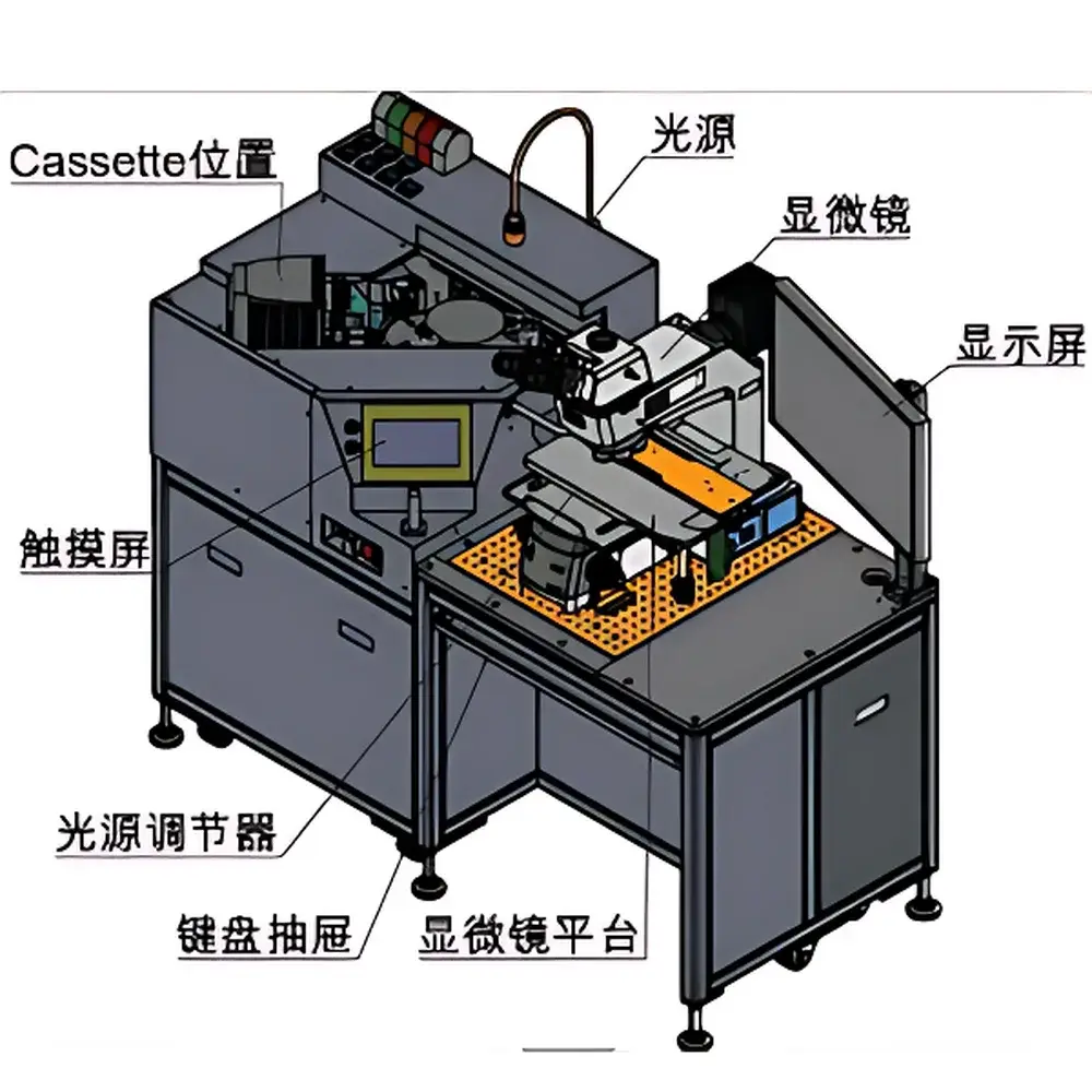
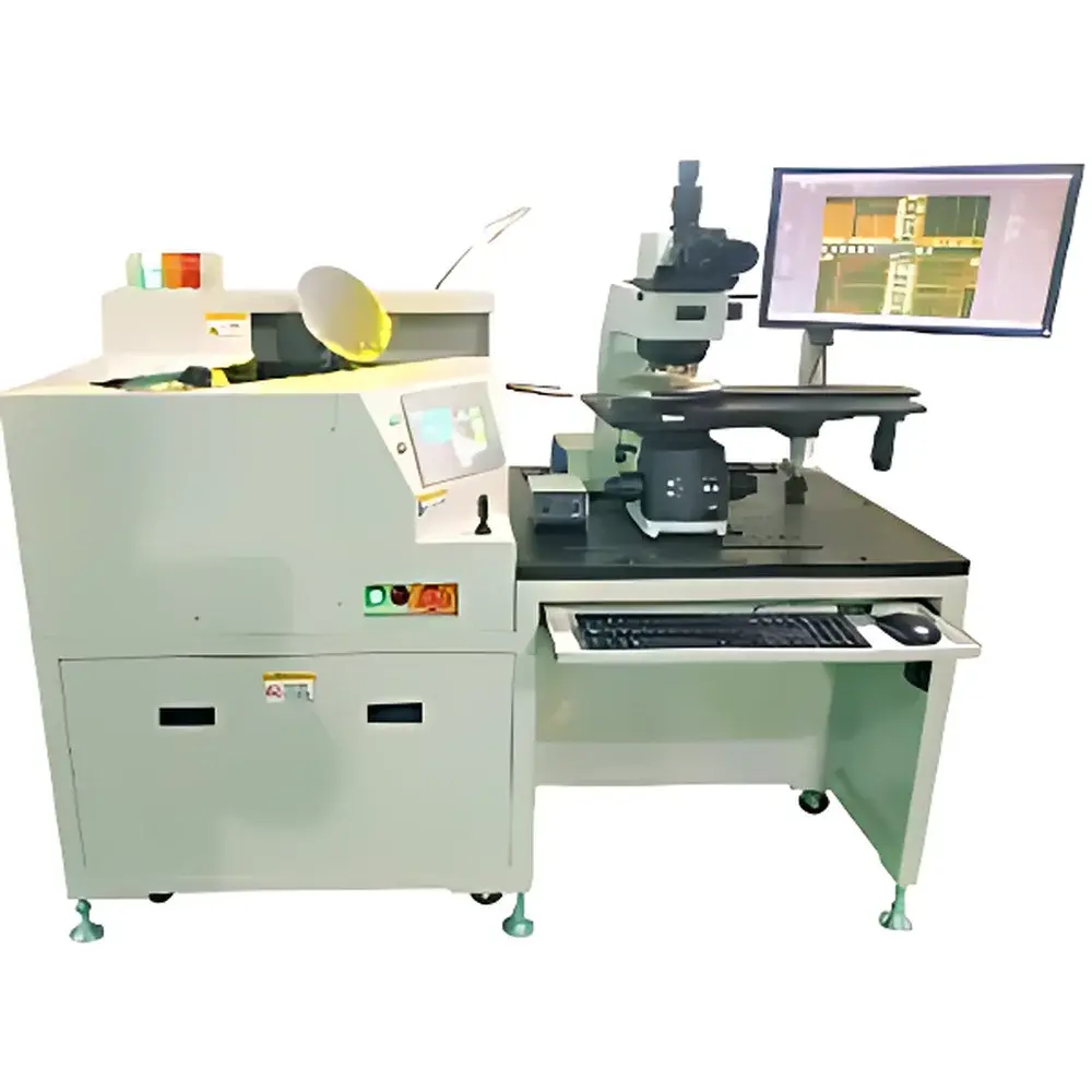
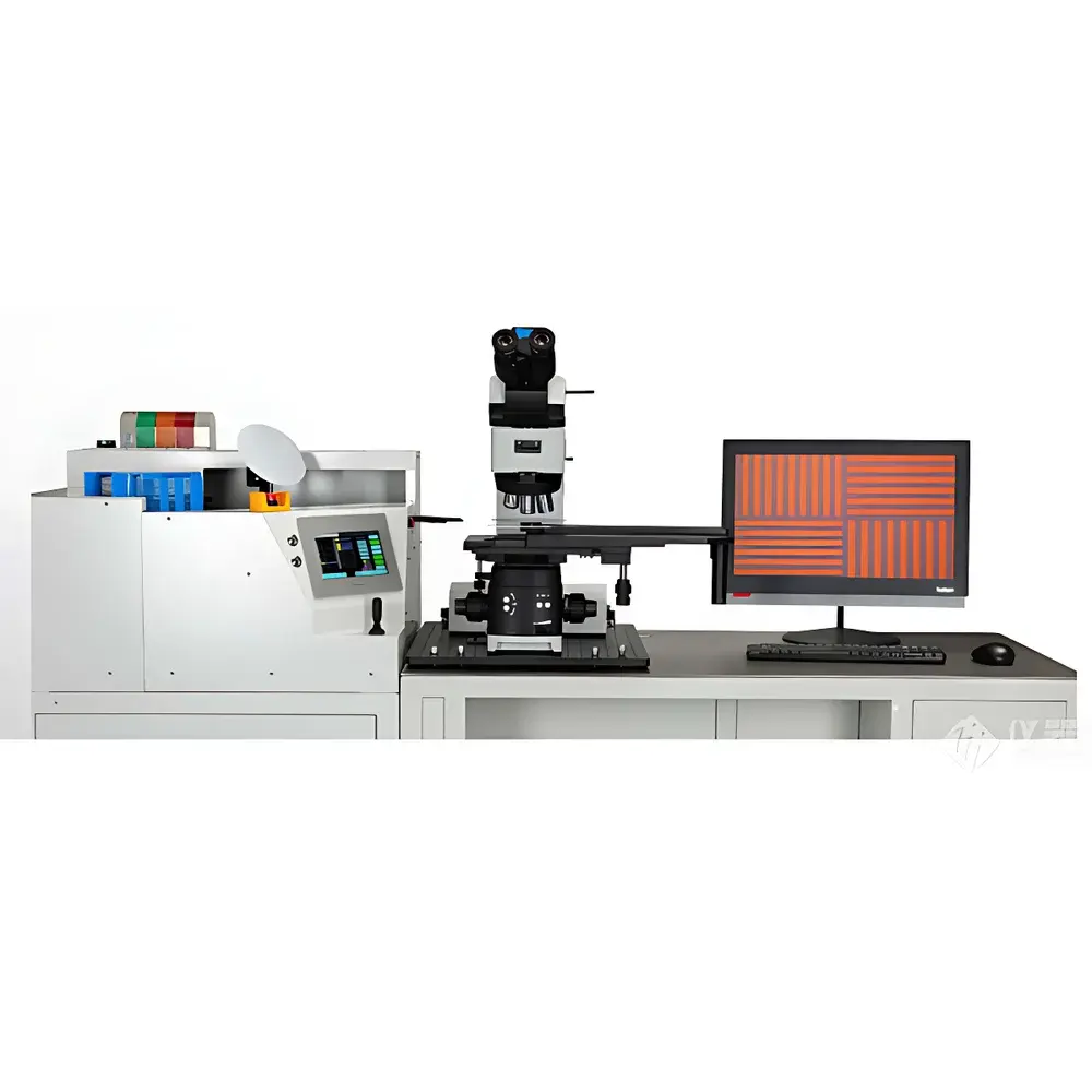
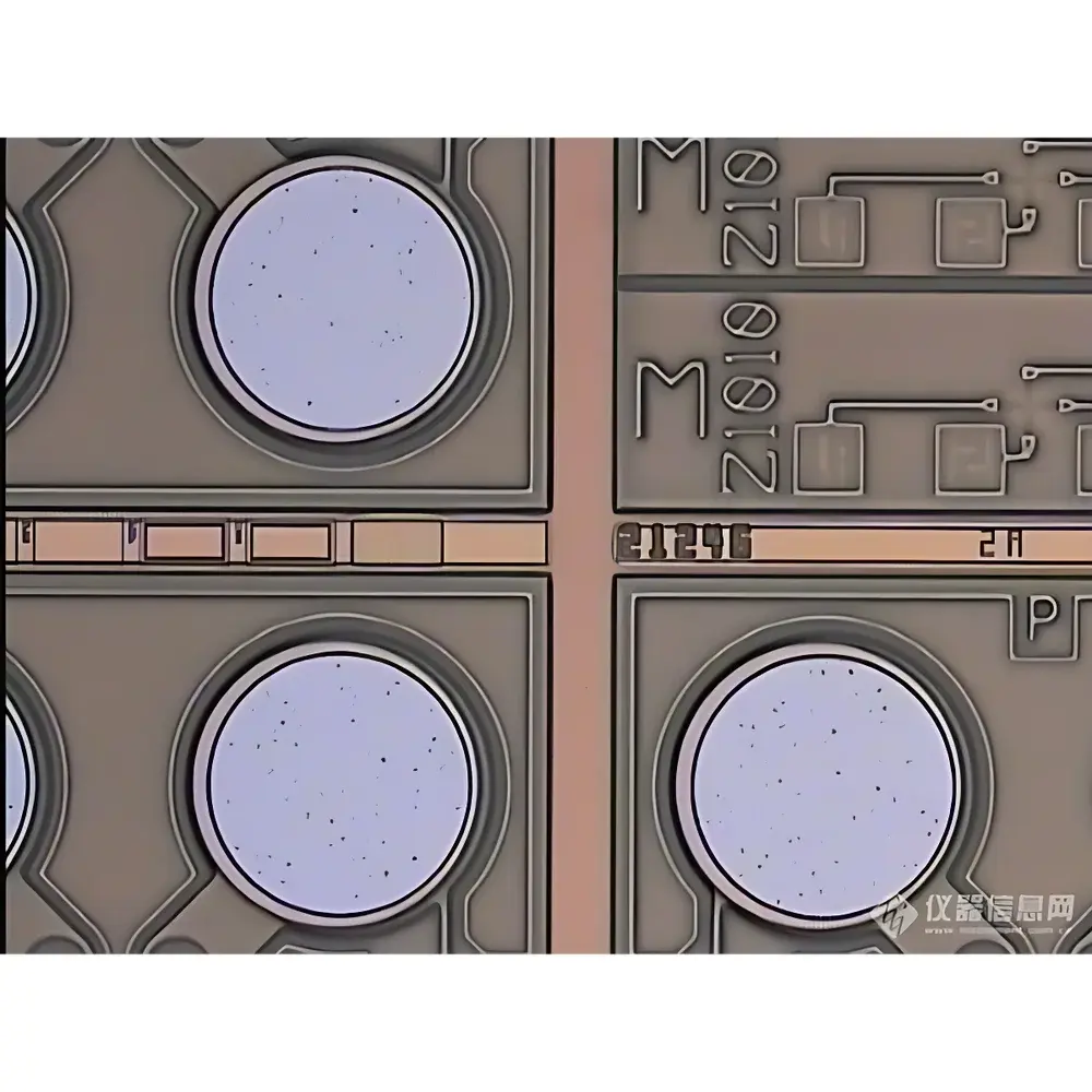
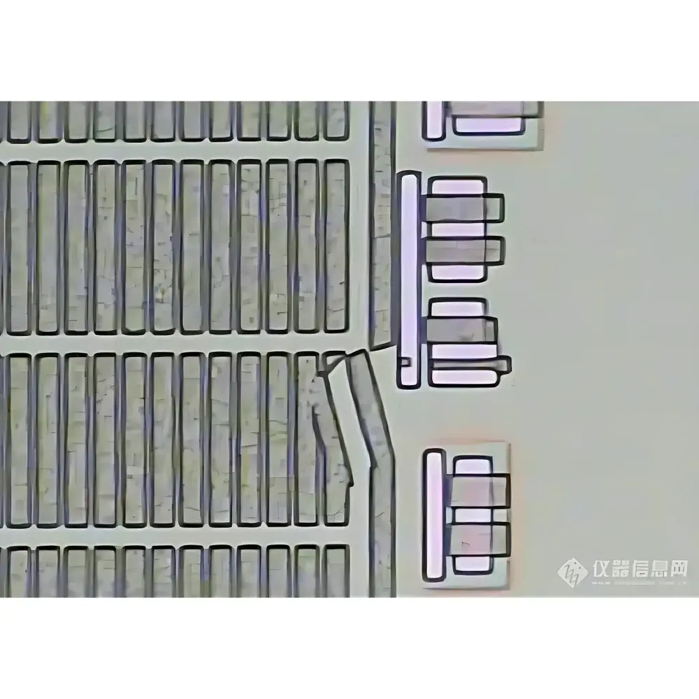
The LEI-TECH LK-BY86 Fully Automated Wafer Handling and Inspection System is an integrated optical inspection platform engineered for high-precision macro-level defect detection and ergonomic manual/semi-automated wafer manipulation in semiconductor fabrication environments. Built upon a rigid mechanical architecture with precision-machined kinematic stages, the system combines vacuum-based wafer clamping, motorized 360° azimuthal rotation, and multi-axis tilt capability to enable comprehensive visual examination of wafer frontside, backside, and edge regions without repositioning or manual flipping. Its core optical inspection methodology relies on bright-field and oblique-angle illumination coupled with high-resolution monochrome imaging—optimized for detecting surface scratches, particles, micro-cracks, edge chipping, and contamination across silicon, SOI, GaAs, and compound semiconductor substrates. Designed for use in cleanroom Class 100–1000 environments, the LK-BY86 supports both inline process monitoring and final outgoing quality assurance workflows in front-end lithography, etch, CMP, and packaging lines.
Key Features
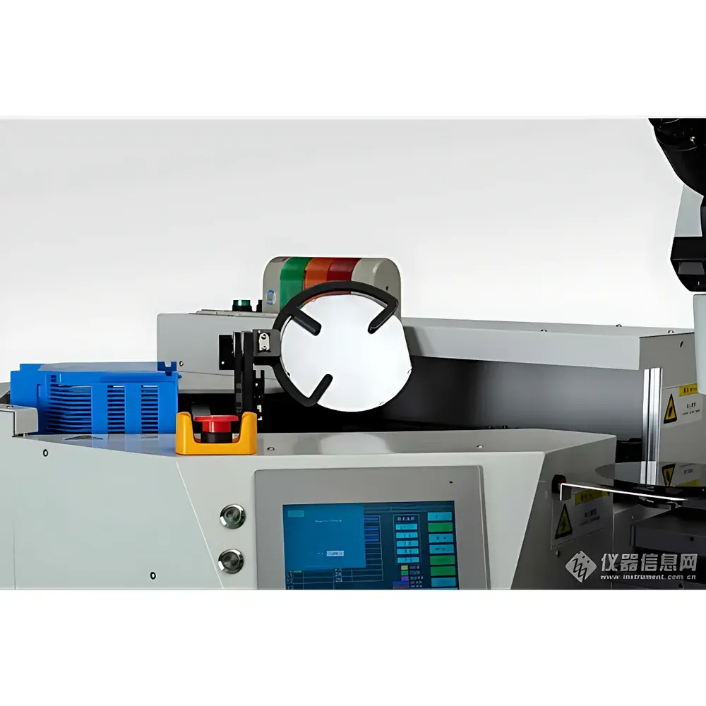
- Triple-diameter compatibility: seamless support for 150 mm (6″), 200 mm (8″), and 300 mm (12″) wafers via adjustable vacuum chuck and centering mechanism
- Full 360° continuous rotation of wafer plane for circumferential macro inspection
- Multi-angle tilt functionality: frontside tilt up to ±70°, backside 1 tilt up to ±90°, and backside 2 tilt up to ±160° — enabling edge-on and near-grazing-angle observation
- Ergonomic manual operation interface with tactile joystick control and intuitive LCD status display showing current inspection mode, sequence index, and real-time parameter settings
- Quick-release vacuum stage with tactile feedback and pressure-sensing interlock for operator safety and repeatable positioning
- Modular mechanical design compliant with SEMI S2/S8 safety standards and ISO 14644-1 cleanroom compatibility requirements
Sample Compatibility & Compliance
The LK-BY86 accommodates standard semiconductor wafers including polished silicon, epitaxial wafers, SOI, SiC, GaN-on-silicon, and quartz substrates. It supports bare wafers, photoresist-coated wafers, and post-CMP wafers with minimal risk of particle generation or mechanical damage due to low-acceleration motion profiles and non-contact optical alignment. The system conforms to SEMI E10 (Definition and Measurement of Equipment Reliability and Availability), SEMI E11 (Equipment Communication Standard), and meets CE marking requirements for machinery safety (2006/42/EC). All electrical components are rated for Class 100 cleanroom operation per ISO 14644-1. Documentation packages include traceable calibration records, FAT/SAT reports, and compliance declarations supporting ISO 9001:2015 and IATF 16949 quality management systems.
Software & Data Management
The embedded inspection software provides configurable inspection protocols with user-defined pass/fail criteria, image capture triggers, and timestamped annotation logging. Each inspection session generates a structured XML metadata file containing wafer ID, operator ID, timestamp, tilt/rotation angles, lighting configuration, and annotated defect coordinates. Audit trails comply with FDA 21 CFR Part 11 requirements when deployed with optional network authentication and electronic signature modules. Data export supports CSV, TIFF, and JPEG formats; integration with MES platforms (e.g., Applied Materials EnVision, PDF Solutions Exensio) is supported via OPC UA or RESTful API interfaces. Firmware updates are delivered via secure HTTPS with SHA-256 signature verification.
Applications
- Pre- and post-lithography macro inspection for resist defects, coating uniformity anomalies, and mask alignment errors
- Post-etch and post-CMP visual verification of pattern fidelity, dishing, erosion, and residual slurry particles
- Final outgoing quality control prior to shipping — verifying absence of handling-induced damage, edge fractures, or backside contamination
- Failure analysis lab support for correlating macro-defect locations with SEM/FIB cross-section targets
- Process tool qualification and preventive maintenance checks for chuck flatness, vacuum integrity, and stage repeatability
FAQ
Does the LK-BY86 support automated defect classification?
No — it is a manual/semi-automated macro inspection station. Defect identification and classification are performed visually by trained operators; no AI-based image analysis engine is included in the base configuration.
Can the system be integrated into a factory automation network?
Yes — optional Ethernet/IP and SECS/GEM communication modules enable integration with host MES and AMHS systems for wafer tracking and recipe synchronization.
What is the recommended maintenance schedule?
Vacuum pump oil change every 2,000 operating hours; optical path cleaning and stage calibration every 6 months or after 500 wafer cycles — documented in the provided PM checklist per ISO 13374 condition monitoring guidelines.
Is remote diagnostics supported?
Yes — built-in VNC server with TLS-encrypted remote access allows LEI-TECH field service engineers to perform real-time troubleshooting and firmware updates under customer authorization.
Does the system meet GLP/GMP documentation requirements?
Yes — with optional 21 CFR Part 11-compliant software package, including electronic signatures, audit trail review tools, and role-based access control logs suitable for regulated semiconductor manufacturing facilities.


