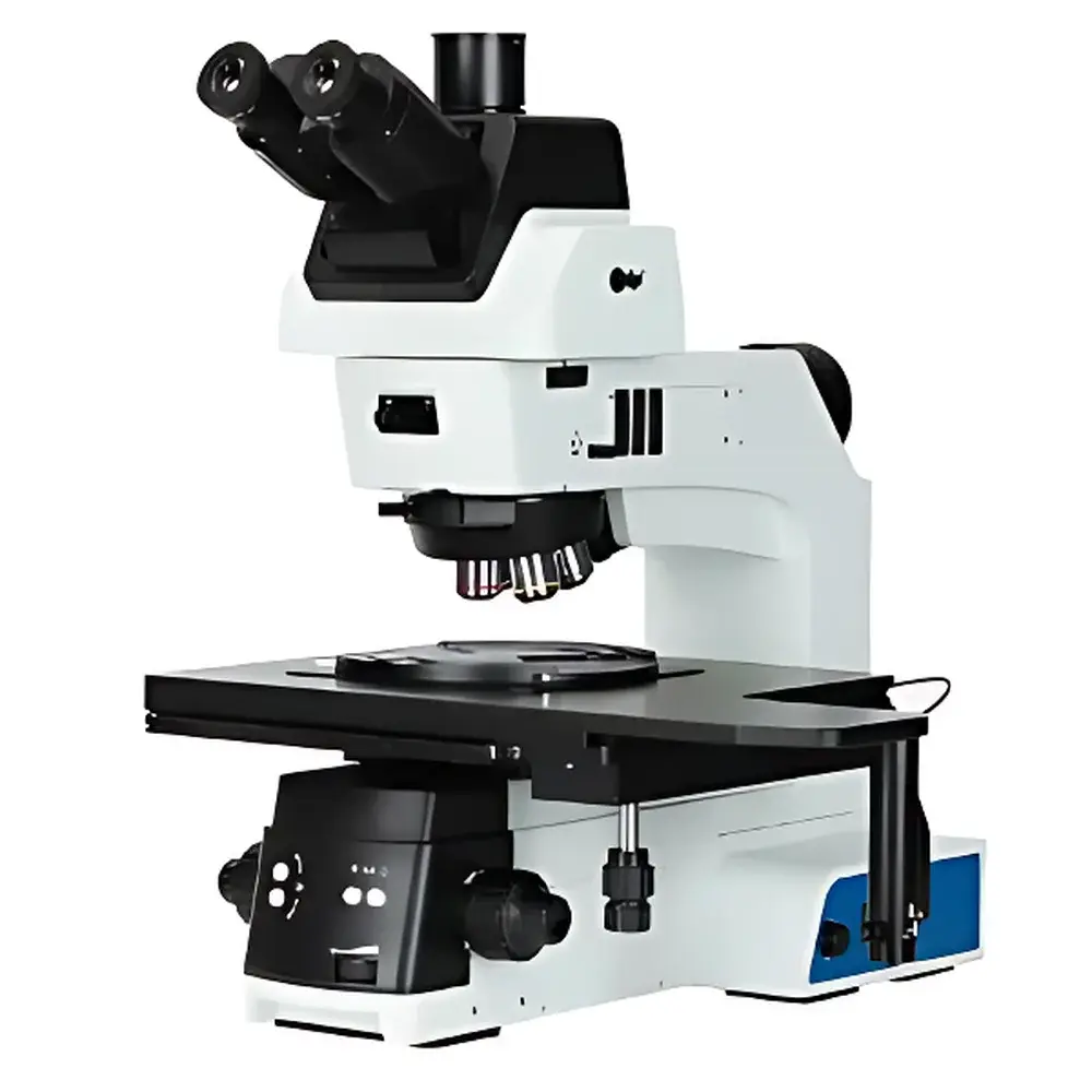
LEI-TECH LK-ZDJY80R Automated Wafer Defect Density Inspection System
| Brand | LEI-TECH |
|---|---|
| Origin | Tianjin, China |
| Manufacturer Type | OEM Manufacturer |
| Product Category | Domestic |
| Model | LK-ZDJY80R |
| Instrument Class | Optical Patterned Defect Inspection System |
| Primary Applications | Wafer process monitoring, outgoing wafer quality control |
| Compatible Wafer Sizes | 4", 6", 8", 12" |
Overview
The LEI-TECH LK-ZDJY80R Automated Wafer Defect Density Inspection System is a high-precision optical inspection platform engineered for quantitative analysis of etch pit morphology and spatial distribution on semiconductor wafers. Based on bright-field and differential interference contrast (DIC) optical imaging principles, the system enables non-destructive, high-magnification surface characterization of crystalline defects—including dislocation-induced etch pits—generated during crystal growth, doping, or mechanical stress in fabrication. Designed specifically for R&D laboratories and front-end process control environments, it delivers traceable, repeatable defect density metrics aligned with industry-standard statistical process control (SPC) requirements. Its modular architecture integrates a motorized XYZ scanning stage, high-resolution monochrome CMOS camera, precision optical microscope, and calibrated illumination subsystem—all synchronized under deterministic real-time control firmware.
Key Features
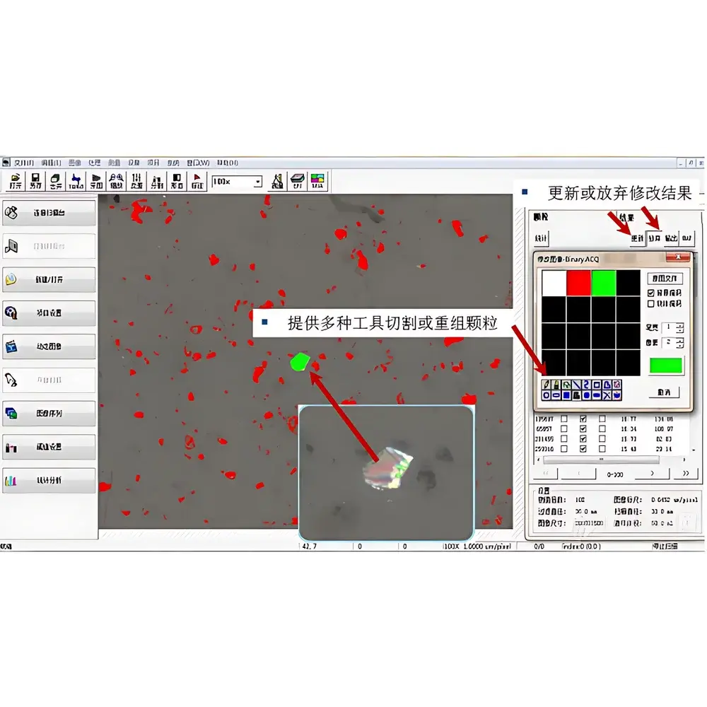
- Fully automated multi-scale scanning: supports rectangular, circular, and user-defined irregular scan regions via four-point ROI definition; blank-area masking reduces redundant image acquisition by up to 35% in typical patterned wafers.
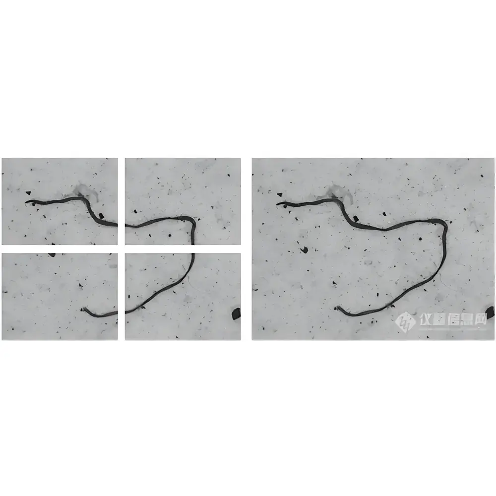
- Adaptive autofocus algorithms: combines polynomial fit compensation for low-magnification fields (≤50×) and multi-frame image fusion for high-magnification operation (≥200×), maintaining sub-micron focus stability across thermal drift and stage motion.
- Comprehensive defect quantification engine: calculates over 12 morphological parameters per detected feature—including equivalent diameter, projected area, aspect ratio, circularity, convexity, and shape factor—enabling correlation between defect geometry and process variables.
- Dual-mode inspection workflow: full-wafer coverage mode for metrology-grade density mapping, and statistically robust sampling mode (M×N grid or fixed-interval spacing) for rapid inline qualification.
- Configurable pass/fail criteria: users define maximum allowable defect count per cell, enabling automated yield binning and SPC charting compliant with JEDEC JESD22-A108 and SEMI E142 standards.
- Electronic archival with audit trail: all raw images, processed data, metadata (timestamp, operator ID, calibration log), and final reports are stored in encrypted SQLite databases with SHA-256 checksum integrity verification.
Sample Compatibility & Compliance
The LK-ZDJY80R accommodates standard silicon, SiC, GaN, and sapphire wafers ranging from 100 mm (4″) to 300 mm (12″) in diameter, including both polished and etched surfaces. It supports manual and auto-load configurations with vacuum chuck compatibility. All measurement protocols adhere to ISO/IEC 17025 technical competence requirements for calibration traceability, and software architecture complies with FDA 21 CFR Part 11 for electronic records and signatures—featuring role-based access control, immutable audit logs, and electronic signature capture for report approval. System validation documentation (IQ/OQ/PQ) is provided per GMP/GLP laboratory implementation guidelines.
Software & Data Management
The proprietary LEI-Vision™ Analysis Suite (v4.2+) provides a unified GUI for acquisition, analysis, and reporting. Data export supports native .xlsx (with embedded formulas for dynamic recalculations), .csv (UTF-8 encoded), and .tif pyramid format for long-term archival. Batch processing pipelines allow parameterized re-analysis of archived datasets without rescanning. Database queries support SQL-like filtering by defect size range, location coordinates, or time-stamped session ID. All reports include customizable templates conforming to internal QA formats or external customer specifications—including ASTM F39–22-compliant wafer map annotations and USP analytical instrument qualification metadata.
Applications
- Crystal growth optimization: correlating etch pit density (EPD) maps with Czochralski pull rate, annealing temperature, and dopant concentration gradients.
- Epitaxial layer quality assessment: detecting threading dislocations in GaN-on-sapphire heterostructures prior to device fabrication.
- Process change verification: quantifying defect reduction post-introduction of new CMP slurry formulations or lithography hardmask materials.
- Failure analysis root cause tracing: overlaying EPD hotspots with electrical test results (e.g., leakage current maps from wafer probe stations).
- Cross-material applicability: validated for particle dispersion analysis in metal powder compacts (ASTM B822), pigment agglomeration in industrial coatings (ISO 15236), and ceramic grain boundary etch pit enumeration.
FAQ
What wafer handling options are available for 300 mm wafers?
The LK-ZDJY80R supports both manual loading with alignment pins and integration-ready interfaces for SMIF pod or FOUP robotic handlers (custom adapter kits required).
Is the system compatible with cleanroom Class 100 environments?
Yes—the enclosure meets SEMI S2-0215 safety certification and optional HEPA-filtered air purge modules are available for ISO Class 5 compliance.
Can defect classification be trained using custom reference libraries?
The software includes supervised learning modules supporting user-defined training sets; model validation follows ASTM E2777–21 guidelines for binary classifier performance evaluation.
How is system calibration maintained over time?
A NIST-traceable graticule slide and certified step-height standard are included for daily focus and pixel-size verification; annual recalibration services are offered with ISO/IEC 17025-accredited certificates.
Does the software support networked deployment across multiple lab sites?
Yes—centralized database hosting via PostgreSQL server allows concurrent access with granular permission tiers; remote diagnostics and firmware updates are supported over TLS-encrypted connections.


