Zhengye TH11 Fully Automated Online Copper Thickness Measurement System
| Brand | Zhengye |
|---|---|
| Origin | Guangdong, China |
| Manufacturer Type | Direct Manufacturer |
| Regional Classification | Domestic (China) |
| Model | TH11 |
| Price Range | USD 28,000 – 70,000 |
Overview
The Zhengye TH11 Fully Automated Online Copper Thickness Measurement System is an industrial-grade, non-contact eddy current-based thickness measurement platform engineered for real-time, in-line monitoring of copper foil thickness on rigid printed circuit boards (PCBs). Designed for integration into high-volume PCB fabrication lines, the system operates on the principle of high-frequency eddy current impedance analysis—where a precisely calibrated alternating magnetic field induces eddy currents in conductive copper layers; the resulting impedance shift correlates directly with copper thickness, enabling sub-micrometer resolution under controlled environmental and material conditions. Unlike offline handheld gauges or destructive cross-sectioning methods, the TH11 delivers continuous, traceable measurements without interrupting conveyor throughput—making it integral to Statistical Process Control (SPC), MSA (Measurement Systems Analysis), and Industry 4.0-ready smart manufacturing infrastructures.
Key Features
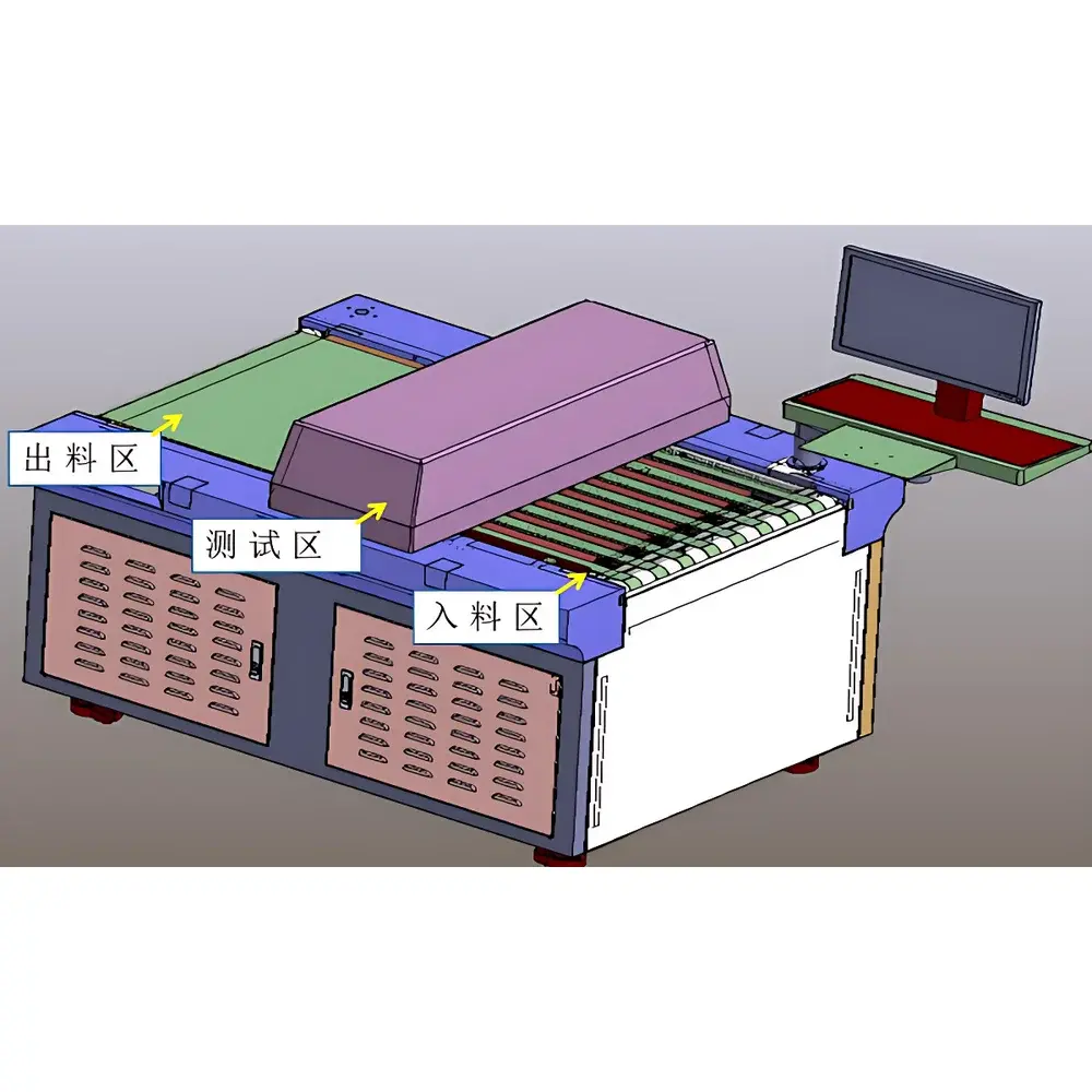
- Fully automated inline operation with seamless integration into standard PCB conveyor systems (300–600 mm belt width compatible); supports PLC-triggered measurement cycles synchronized with board indexing.
- Dual-sided copper thickness acquisition via patented dual-probe kinematic alignment—eliminates manual repositioning and ensures simultaneous top/bottom layer evaluation with <±0.3 µm repeatability (per ASTM B487-22 Annex A2).
- Integrated Fischer PC2 main controller with ERCU N-surface eddy current probe—factory-calibrated for Cu-on-epoxy, Cu-on-PI, and electroplated Cu substrates; supports automatic temperature compensation (15–35 °C operating range).
- Robust mechanical architecture featuring IP54-rated enclosure, anti-vibration damping mounts, and ESD-safe handling modules compliant with IPC-A-600G section 1.5.2 for cleanroom-adjacent deployment.
- Real-time pass/fail logic engine with configurable tolerance bands (user-definable ±X µm per layer); immediate visual/audio alerts and digital output signals for upstream process intervention.
Sample Compatibility & Compliance
The TH11 accommodates rigid PCBs with total thickness ranging from 0.050 mm to 12.0 mm—including single-layer FR-4, multilayer sequential build-ups, HDI structures, and metal-core boards. It measures electrodeposited and rolled copper foils from 5 µm to 120 µm nominal thickness, with validated performance across surface roughness (Ra ≤ 1.2 µm) and dielectric constant variations (εr = 3.2–4.8). System compliance includes ISO/IEC 17025:2017 methodology traceability (via NIST-traceable reference standards), adherence to IPC-TM-650 2.2.17.1 for non-destructive copper thickness verification, and full audit readiness for GLP/GMP environments—including electronic signature support and 21 CFR Part 11-compliant data integrity protocols.
Software & Data Management
The embedded TH11 Control Suite (v3.2+) provides web-accessible HMI with role-based user permissions (Operator, Technician, Admin). All measurements are timestamped, geotagged (by station ID), and stored in encrypted SQLite databases with automatic daily backup to network shares or cloud S3 buckets. Raw impedance waveforms, layer-wise thickness histograms, SPC control charts (X̄-R, Cpk), and MSA reports (Gage R&R, bias, linearity) are exportable in CSV, PDF, and XML formats. RESTful API enables bidirectional integration with MES (e.g., Siemens Opcenter, Rockwell FactoryTalk) and ERP platforms (SAP, Oracle)—supporting ODBC, MQTT, and OPC UA communication stacks.
Applications
- In-process verification during pattern plating and full-board electroplating stages to prevent over-/under-copper conditions prior to etching.
- Final QA gate for automotive and aerospace PCBs requiring IPC Class 3 conformance (IPC-6012DS) and AS9100-relevant thickness uniformity reporting.
- Process validation for HDI microvia filling consistency and buried copper layer integrity in 10+ layer stack-ups.
- Root cause analysis of blistering, delamination, or solder mask adhesion failure linked to localized copper thickness deviation (>±8% from nominal).
- Supporting PPAP documentation packages with automated generation of IMDS-compatible material thickness records.
FAQ
Does the TH11 require periodic recalibration with physical standards?
Yes—calibration must be performed at least once per shift using NIST-traceable copper foil standards (certified thickness ±0.1 µm); the system logs all calibration events with operator ID and timestamp.
Can the TH11 measure copper thickness through solder mask or silkscreen?
No—it requires direct exposure of the copper surface; cured solder mask (≤35 µm) may be accommodated only if its dielectric properties are pre-characterized and compensated in the measurement algorithm.
Is offline data analysis supported without the host PC?
Yes—the onboard controller stores up to 12 months of compressed measurement history; USB export enables offline review using the free TH11 Data Viewer application (Windows/macOS/Linux).
What maintenance intervals are recommended for the ERCU probe?
Probe tip inspection and cleaning every 200 operating hours; full probe recalibration and cable integrity test every 6 months or after 10,000 measurement cycles—whichever occurs first.
How does the system handle warped or bowed PCBs?
Integrated laser triangulation height mapping (±5 µm accuracy) dynamically adjusts probe lift-off distance in real time; maximum allowable bow is ±0.8 mm across 300 mm diagonal.


