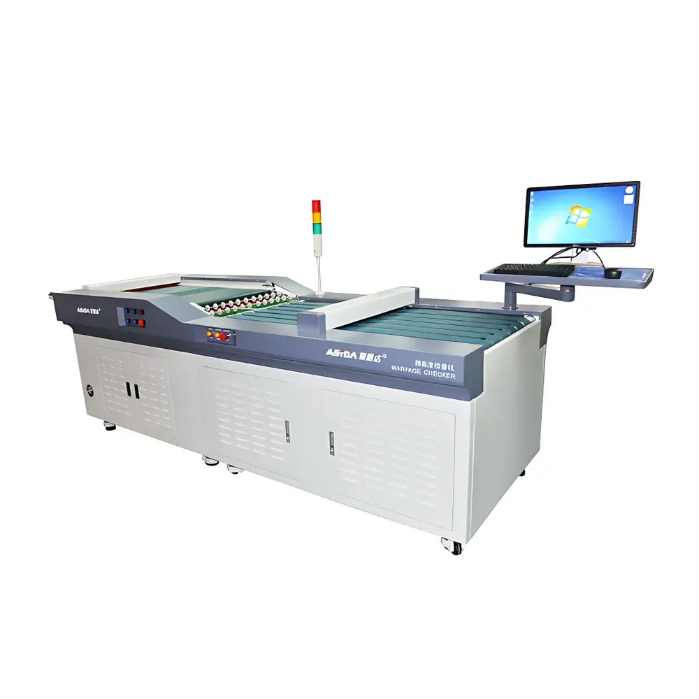
Asida QQ1000 PCB Warpage Inspection System
| Brand | Asida |
|---|---|
| Origin | Guangdong, China |
| Manufacturer Type | Authorized Distributor |
| Country of Origin | China |
| Model | QQ1000 |
| Pricing | Available Upon Request |
Overview
The Asida QQ1000 PCB Warpage Inspection System is a non-contact, automated optical metrology platform engineered for high-throughput, quantitative measurement of board-level warpage in rigid and flexible printed circuit boards (PCBs), copper-clad laminates (CCL), and substrate panels. It employs triangulation-based laser displacement sensing coupled with high-resolution CCD imaging to reconstruct the full 3D surface topography of flat-panel components. Unlike manual dial indicator or pin-based methods, the QQ1000 captures spatial deviation across the entire board surface—measuring bow, twist, and localized curvature per IPC-TM-650 2.4.22 and JEDEC JESD22-B112A standards. Designed for integration into final QA stations or inline process monitoring points, the system delivers repeatable sub-micron vertical resolution and supports real-time pass/fail classification based on user-defined GD&T tolerances.
Key Features
- Non-contact 3D surface profiling using dual-axis laser displacement sensors and industrial-grade CCD optics
- Automated warpage quantification per IPC-defined metrics: maximum bow (mm), maximum twist (mm), and sagittal height deviation (µm)
- Configurable board dimension input (L × W × T) with unlimited recipe storage for multi-product environments
- Real-time OK/NG decision logic with configurable tolerance bands for bow, twist, and composite warpage index
- Modular mechanical architecture enabling seamless integration with conveyor lines, AOI stations, or automated material handling systems
- Integrated data logging with timestamped warpage maps, statistical process control (SPC) output, and CSV/PDF export capabilities
- Intuitive Windows-based GUI with multilingual support (English, Simplified Chinese, Korean), no specialized metrology training required
- Firmware-upgradable software architecture supporting custom algorithm deployment and customer-specific reporting templates
Sample Compatibility & Compliance
The QQ1000 accommodates rigid PCBs from 50 mm × 50 mm up to 600 mm × 500 mm, including FR-4, polyimide, metal-core, and HDI substrates with thicknesses ranging from 0.2 mm to 6.0 mm. It complies with IPC-A-600G Class 2/3 visual acceptance criteria for warpage-related defects and supports audit-ready documentation aligned with ISO 9001:2015 and IATF 16949 quality management requirements. Measurement traceability follows NIST-traceable calibration protocols; system validation reports include MSA (Gage R&R) studies per AIAG MSA 4th Edition. Optional 21 CFR Part 11-compliant software modules are available for regulated medical device PCB manufacturing environments.
Software & Data Management
The proprietary AsidaVision™ software provides real-time 3D warpage visualization, cross-sectional profile slicing, and comparative overlay analysis between nominal CAD geometry and measured surface data. All inspection records—including raw sensor data, thermal drift compensation logs, operator ID, and environmental metadata (ambient temperature/humidity)—are stored in an encrypted SQLite database with configurable retention policies. SPC dashboards generate Cp/Cpk indices, X-bar-R charts, and outlier detection alerts. Data export supports industry-standard formats (CSV, XML, PDF) and integrates via OPC UA or RESTful API with MES platforms such as Siemens Opcenter, Rockwell FactoryTalk, or Cimetrix CIMConnect.
Applications
- Final outgoing quality assurance for automotive, aerospace, and server-grade PCBs prior to packaging
- In-process warpage monitoring after lamination, solder mask application, or reflow soldering
- Process capability assessment during new product introduction (NPI) and design for manufacturability (DFM) validation
- Root cause analysis of thermal stress-induced deformation in lead-free assembly processes
- Supplier qualification audits requiring objective, repeatable warpage benchmarking against contractual specifications
- Failure analysis correlation with BGA voiding, delamination, or solder joint fatigue in reliability testing
FAQ
What warpage metrics does the QQ1000 report?
It calculates maximum bow (peak-to-valley deviation along length/width), maximum twist (diagonal angular distortion), and composite warpage index (RMS surface deviation) per IPC-TM-650 2.4.22.
Can it measure warped flex or rigid-flex PCBs?
Yes—provided the flex region is mechanically stabilized during scanning; optional vacuum fixture kits are available for low-stiffness substrates.
Is calibration required before each shift?
No. The system performs automatic zero-point compensation at startup and includes temperature-drift correction algorithms validated over 15–35°C ambient range.
Does it support statistical process control (SPC) reporting?
Yes. Built-in SPC engine generates control charts, capability indices, and alarm-triggered email notifications via SMTP.
How is measurement traceability maintained?
Each unit ships with a factory calibration certificate referencing NIST-traceable standards; annual recalibration services include uncertainty budget documentation per ISO/IEC 17025.
Related Products