X-ray Fluorescence Coating Thickness Analyzer and Material Composition Analyzer XDLM-PCB210
| Origin | Germany |
|---|---|
| Manufacturer Type | Authorized Distributor |
| Origin Category | Imported |
| Model | XDLM-PCB210 |
| Pricing | Available Upon Request |
Overview
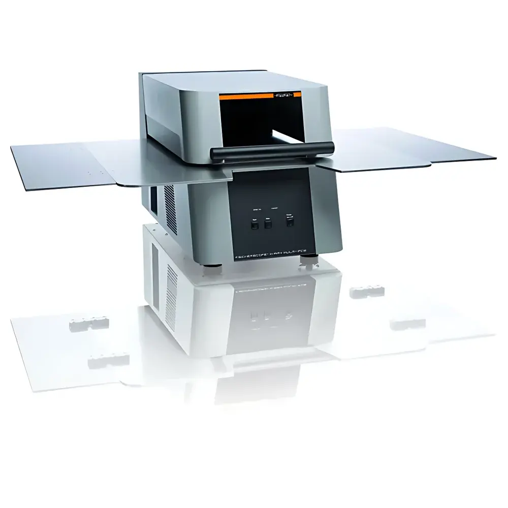
The XDLM-PCB210 is a benchtop energy-dispersive X-ray fluorescence (EDXRF) spectrometer engineered for non-destructive, high-precision measurement of multi-layer metallic coatings and quantitative elemental analysis of solid and liquid samples. Operating on the principle of characteristic X-ray emission following primary X-ray excitation, the instrument enables simultaneous determination of coating thicknesses (down to sub-micrometer resolution) and elemental composition (from Na to U) without sample preparation. Designed specifically for high-mix, low-volume production environments—particularly in printed circuit board (PCB) manufacturing—the system delivers traceable, repeatable results compliant with ISO 3497, ASTM B568, and IPC-4552A standards for electroplated copper, nickel, gold, tin, and solder mask (e.g., green solder resist) thickness verification.
Key Features
- Single-software platform supporting both coating thickness quantification and bulk/solution-phase elemental analysis—eliminating workflow fragmentation across plating line QC, lab R&D, and incoming material inspection.
- Selectable X-ray source configurations: microfocus tungsten anode tube with either beryllium (Be) or glass exit window, optimized for low-Z element sensitivity (e.g., C, O, Al in solder mask) or high-intensity excitation of mid-to-high Z elements (e.g., Cu, Ni, Au).
- Modular detector options: proportional counter (PC), silicon PIN diode, or high-resolution silicon drift detector (SDD), enabling trade-off optimization between count rate, energy resolution (<130 eV at Mn Kα for SDD), and cost per application.
- Motorized, software-controlled collimator turret with four apertures (including 50 × 50 µm fine-spot mode) and up to six programmable primary beam filters—enabling automated adaptation to diverse sample geometries, matrix effects, and inter-element interference scenarios.
- Integrated XYZ motorized stage with optical microscope alignment (10× magnification) and auto-focus capability, ensuring precise positioning over vias, traces, pads, and irregular PCB features.
Sample Compatibility & Compliance
The XDLM-PCB210 accommodates rigid flat samples up to 300 × 300 mm and thicknesses ≤ 50 mm—including FR-4 substrates, flex circuits, ceramic packages, and metal stampings. It supports direct analysis of plating bath solutions (via sealed cuvettes), solder pastes, and conductive inks. All measurement routines are fully traceable and support audit-ready reporting aligned with GLP and GMP requirements. Data integrity is maintained via built-in electronic signatures, time-stamped audit trails, and optional 21 CFR Part 11 compliance modules. Calibration stability is verified daily using onboard reference standards; long-term drift correction is enabled through internal reference peak monitoring (e.g., Rh Kα from tube anode).
Software & Data Management
Fischer’s proprietary FISCHERSCOPE® XDL software provides intuitive workflow-guided operation—from method creation and calibration to batch reporting and SPC charting. Measurement methods store full spectral acquisition parameters (voltage, current, live time, filter/collimator selection), background subtraction algorithms (Compton normalization), and fundamental parameter (FP) or empirical calibration models. Raw spectra are stored in standardized .spc format; reports export to PDF, CSV, and XML for LIMS integration. Multi-user role-based access control ensures secure configuration management, while version-controlled method libraries facilitate cross-site standardization across global manufacturing facilities.
Applications
- PCB manufacturing: Cu plating thickness in microvias (≤ 10 µm), ENIG (electroless nickel immersion gold) layer stack quantification, solder mask thickness uniformity mapping, and Cu foil weight validation.
- Electroplating process control: real-time monitoring of bath chemistry (Ni²⁺, Co²⁺, Zn²⁺, cyanide complexes) via liquid cell analysis; detection limits < 1 ppm for key metals.
- Aerospace & automotive: measurement of Cr(VI)/Cr(III) passivation layers on aluminum alloys, Zn-Ni alloy coatings on fasteners, and thermal barrier coating (TBC) elemental homogeneity.
- Jewelry & precious metals: karat verification of Au-Ag-Cu alloys, detection of Rh or Pd plating on white gold, and hallmark authenticity screening.
- Semiconductor packaging: thickness and stoichiometry of NiP, Ag, and SnAgCu UBM (under-bump metallization) layers.
FAQ
Can the XDLM-PCB210 measure coatings on curved or non-planar surfaces?
Yes—using optional height-sensing Z-axis compensation and custom-defined measurement grids, the system maintains focal distance accuracy within ±5 µm across radii down to 5 mm.
Is it possible to analyze solder paste composition before reflow?
Yes—using a sealed quartz cuvette and optimized low-voltage excitation, the instrument quantifies Sn, Pb, Ag, Cu, and Bi content with ±0.2 wt% repeatability (n=10).
Does the system support ISO/IEC 17025 accredited calibration?
Yes—Fischer provides NIST-traceable certified reference materials (CRMs) and on-site calibration verification services meeting ILAC-MRA requirements.
How is spectral interference between overlapping peaks (e.g., S Kα and Pb Mα) resolved?
Through deconvolution using factory-installed peak fitting algorithms based on physically modeled line shapes and detector response functions—not simple region-of-interest integration.
What maintenance is required beyond annual recalibration?
Only periodic cleaning of the Be window and collimator aperture; no consumables or gas refills are needed—the SDD operates at Peltier-cooled temperatures without liquid nitrogen or mechanical cryocoolers.


