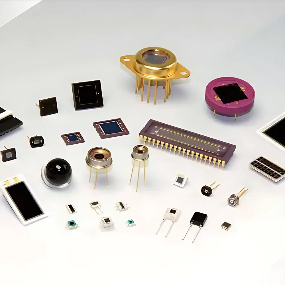
Hamamatsu Silicon Photodiode Series
| Brand | Hamamatsu |
|---|---|
| Origin | Japan |
| Manufacturer Type | Original Equipment Manufacturer (OEM) |
| Import Status | Imported |
| Model Range | Full Series |
| Price Range | USD 0 – 7,000 |
Overview
Hamamatsu Silicon Photodiodes are precision semiconductor photodetectors engineered for high-fidelity optical signal conversion across a broad spectral range—from 190 nm (deep ultraviolet) to 1100 nm (near-infrared). Based on optimized silicon p–n or p–i–n junction architectures, these devices operate on the principle of the internal photoelectric effect: incident photons generate electron–hole pairs within the depletion region, producing a photocurrent linearly proportional to irradiance under reverse-biased or photovoltaic operation. Designed for metrological-grade stability and repeatability, they serve as primary sensing elements in calibrated radiometric, spectrophotometric, and fluorometric systems—particularly where low dark current, fast temporal response (1 GΩ) are critical performance requirements.
Key Features
- Wide Spectral Responsivity: Peak responsivity between 200–1000 nm; enhanced UV response via shallow-junction or quartz-window packaging; optional AR-coating for >95% quantum efficiency at target wavelengths.
- Low-Noise Performance: Typical dark current <100 pA (at 25°C, -5 V bias); noise-equivalent power (NEP) as low as 1 × 10⁻¹⁵ W/√Hz, enabling detection of sub-picoamp photocurrents in lock-in or transimpedance configurations.
- High Speed & Linearity: Rise/fall times down to 3 ns (depending on active area and capacitance); linearity deviation <±0.2% over six decades of irradiance (10−12–10−6 W/cm²).
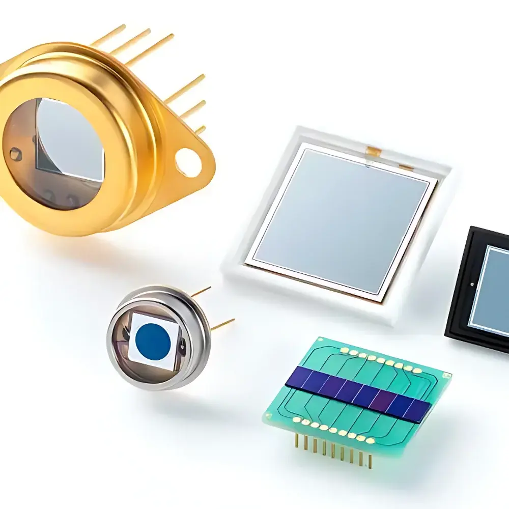
- Robust Packaging Options: Hermetically sealed metal (TO-5, TO-8), ceramic (LCC), and surface-mount (SMD) packages; customizable window materials (fused silica, sapphire, borosilicate); optional integrated thermistors for temperature compensation.
- OEM Integration Support: Custom active-area geometries (round, square, annular), tailored spectral filtering (integrated bandpass/ND filters), and hybrid modules with integrated transimpedance amplifiers (TIA) or logarithmic converters.
Sample Compatibility & Compliance
These photodiodes are compatible with standard optical bench setups, fiber-coupled interfaces (SMA, FC/PC), and vacuum-compatible environments (metal/ceramic variants). All devices comply with JEDEC JESD22-A108 reliability standards for temperature cycling and humidity exposure. Hamamatsu’s manufacturing processes adhere to ISO 9001 and IATF 16949 quality management systems. For regulated applications—including clinical analyzers, environmental monitoring instruments, and pharmaceutical QC equipment—the diodes support traceable calibration per NIST-traceable reference standards and are documented for GLP/GMP-compliant system integration. Device-level documentation includes full spectral responsivity curves, dark current vs. temperature plots, and capacitance vs. reverse voltage data—essential for uncertainty budgeting in ISO/IEC 17025-accredited laboratories.
Software & Data Management
While the silicon photodiodes themselves are passive analog sensors, Hamamatsu provides comprehensive system-level support for digital integration. Compatible with industry-standard DAQ platforms (NI PXI, Keysight U2300A), the diodes interface seamlessly with Hamamatsu’s C12791-series photoreceiver modules and C13492-series multichannel detector arrays—each featuring onboard 16-bit ADCs, real-time baseline correction, and USB/Ethernet communication. Firmware supports SCPI command sets and LabVIEW/VB.NET/.NET SDKs. All acquisition software implements audit-trail logging compliant with FDA 21 CFR Part 11 requirements when deployed in validated environments. Calibration certificates include measurement uncertainty statements per ISO/IEC 17025 Annex A.5, with traceability to PTB (Physikalisch-Technische Bundesanstalt) and NIST reference detectors.
Applications
- Scientific Instrumentation: Beam monitoring in UV-Vis-NIR spectrophotometers; reference channel detection in FTIR interferometers; fluorescence lifetime decay analysis (TCSPC-compatible).
- Medical & Life Sciences: Pulse oximetry sensor arrays; flow cytometry scatter/fluorescence detection; UV disinfection dose monitoring (254 nm Hg-line).
- Industrial Metrology: Laser power stabilization feedback loops; wafer inspection illumination uniformity mapping; colorimetric sensor calibration standards.
- Optical Communications: Low-speed receiver front-ends (≤1 Gbps) in PON and industrial fiber links; optical power meters with ±0.5% linearity accuracy.
- Environmental Sensing: Solar UV index monitoring (UV-A/B), particulate matter (PM2.5) nephelometry, and gas absorption spectroscopy (e.g., O3, NO2) using LED-based differential optical absorption systems.
FAQ
What is the typical shunt resistance for Hamamatsu silicon photodiodes?
Standard devices exhibit shunt resistance >1 GΩ at 25°C and –5 V bias; low-noise variants exceed 10 GΩ. Exact values are provided in individual datasheets and vary with active area and junction design.
Can these photodiodes be used in photovoltaic mode without external bias?
Yes. All models support zero-bias (photovoltaic) operation, though response speed and linearity are optimized under reverse bias (typically –1 V to –10 V).
Do you provide NIST-traceable calibration certificates?
Yes—calibration services are available for absolute responsivity (A/W) at discrete wavelengths (250–1050 nm) with expanded uncertainty ≤1.2% (k=2), traceable to NIST SRM 2271 and PTB reference detectors.
Are custom spectral filters integrated directly onto the die?
Yes. Hamamatsu offers thin-film interference filters deposited directly on the silicon surface or on the package window, including bandpass, longpass, and notch configurations with edge steepness OD5.
What is the maximum permissible optical power density before damage?
For continuous-wave illumination, the damage threshold is typically 100 mW/mm² for uncooled devices with standard AR coating; pulsed operation (ns–ps) requires evaluation per pulse energy, spot size, and repetition rate—consult application engineering for laser-induced damage threshold (LIDT) validation reports.


