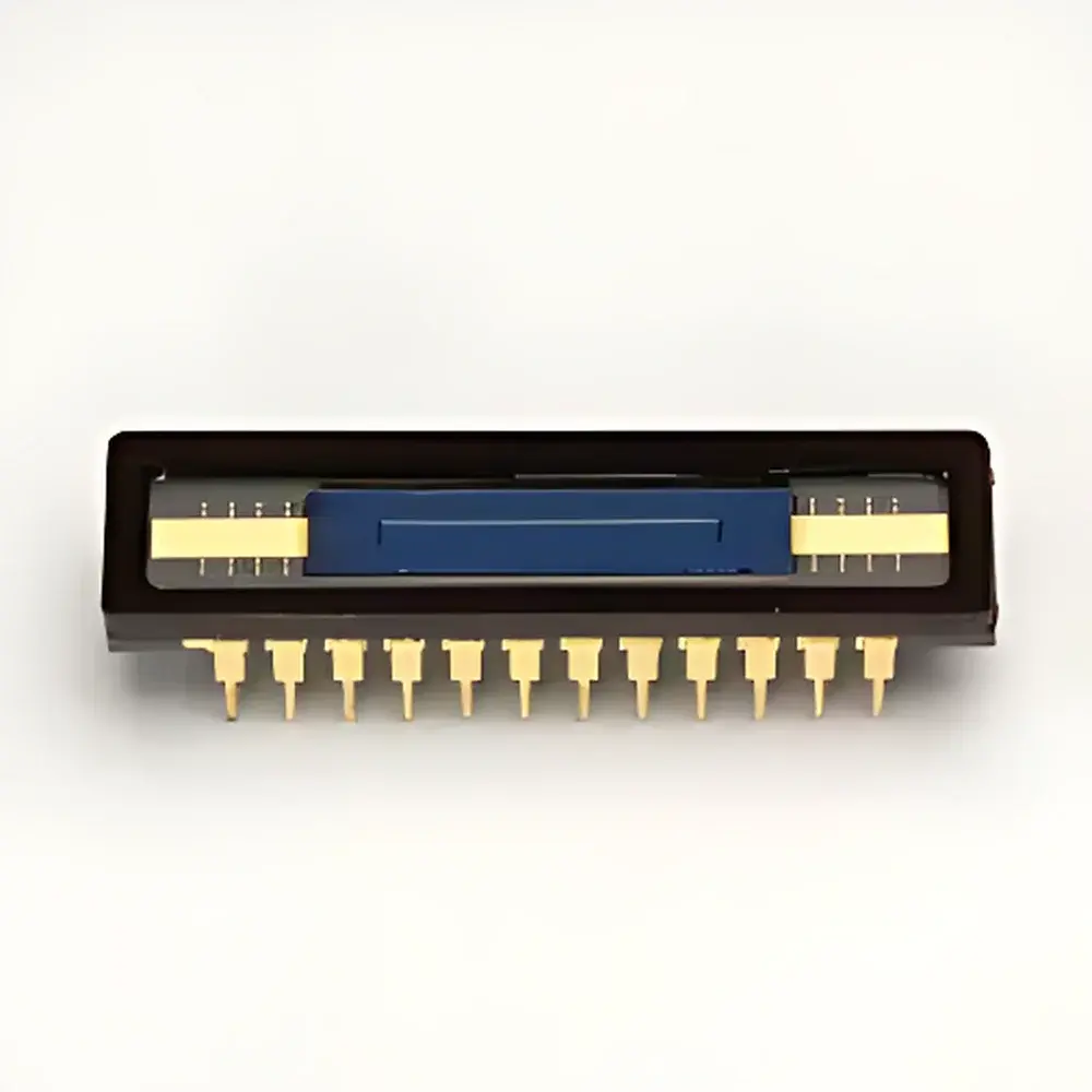
Hamamatsu S11510-1006 Infrared-Enhanced FFT-CCD Area Image Sensor
| Brand | Hamamatsu |
|---|---|
| Origin | Japan |
| Manufacturer Type | Original Equipment Manufacturer (OEM) |
| Product Category | Imported Optical Component |
| Model | S11510-1006 |
| Component Type | Optical Sensor |
| Quantum Efficiency | 40% @ 1000 nm |
| Active Area | 14.336 × 0.896 mm |
| Pixel Pitch | 14 µm |
| Pixel Count | 1024 × 64 |
| Pixel Size | 14 × 14 µm |
| Spectral Range | 200–1100 nm |
| Full-Well Capacity | 60 ke⁻ (typ.) |
| Dark Current | 50 e⁻/pixel/s (typ., Ta = 25 °C) |
| Read Noise | 6 e⁻ rms (typ.) |
| Frame Rate | 189.0 fps (full-line binning, typ.) |
| Package | Ceramic |
| MPP Operation Support | Yes |
| Compatible Driver Board | C11287 |
Overview
The Hamamatsu S11510-1006 is a back-illuminated, frame-transfer charge-coupled device (FFT-CCD) area image sensor engineered for high-sensitivity detection in the near-infrared (NIR) spectrum—specifically optimized for spectroscopic applications requiring robust performance from 200 nm to 1100 nm. Unlike conventional front-illuminated CCDs, the S11510-1006 incorporates a proprietary laser-micromachined MEMS structure on its thinned silicon backside, significantly enhancing quantum efficiency (QE) in the NIR region—reaching 40% at 1000 nm. This architectural innovation enables superior photon collection efficiency beyond 800 nm, making it especially suitable for low-light analytical instruments such as Raman spectrometers, NIR photometers, and UV-Vis-NIR absorption systems where spectral fidelity and signal integrity are critical.
Key Features
- Infrared-enhanced QE: 40% at 1000 nm, enabled by back-illumination and MEMS-based anti-reflection microstructure
- High full-well capacity of 60 ke⁻ (typ.), supporting wide dynamic range measurements without saturation in high-flux conditions
- Low read noise of 6 e⁻ rms (typ.) and dark current of 50 e⁻/pixel/s (typ., 25 °C), ensuring high signal-to-noise ratio (SNR) in long-exposure or low-intensity applications
- Full-line binning capability: merges all 64 vertical pixels into a single effective row (1024 × 1), increasing sensitivity and frame rate up to 189.0 fps—without external analog summation circuitry
- Back-illuminated architecture with MPP (Multi-Pinned Phase) operation mode for reduced dark current and improved charge transfer efficiency
- Pitch-matched pinout and identical drive timing to legacy S10420-01, enabling drop-in replacement in existing optical instrument designs
- Ceramic LCC package with hermetic sealing, rated for stable operation under laboratory-grade thermal and mechanical conditions
Sample Compatibility & Compliance
The S11510-1006 is designed for integration into OEM optical instrumentation where regulatory traceability and environmental stability are essential. Its ceramic packaging meets JEDEC J-STD-020 moisture sensitivity level (MSL) requirements for reflow-compatible assembly. While the sensor itself is not certified to ISO/IEC 17025 or FDA 21 CFR Part 11, its electrical and optical specifications support compliance pathways when embedded in end-user systems validated under GLP, GMP, or IEC 61000-4 electromagnetic compatibility standards. The device operates within standard laboratory ambient conditions (Ta = 15–35 °C, RH < 70%, non-condensing), and its spectral response aligns with ASTM E308-22 for colorimetric and photometric calibration workflows.
Software & Data Management
As a bare sensor component, the S11510-1006 does not include onboard firmware or embedded software. It interfaces exclusively via analog video output (differential or single-ended) synchronized to external clocking signals generated by compatible driver boards such as the Hamamatsu C11287. System-level data acquisition relies on host-side ADC digitization, typically implemented using PCIe-based digitizers or FPGA-based acquisition platforms. When integrated into spectrometer systems compliant with USP or ISO/IEC 17025, users must implement audit-trail-capable software (e.g., LabVIEW with DIAdem, MATLAB with Data Acquisition Toolbox, or custom Qt/C++ applications) to log timestamped raw frames, exposure parameters, temperature metadata, and calibration coefficients. Bin-mode configuration and gain settings are controlled externally through timing register programming—enabling reproducible, version-controlled acquisition protocols.
Applications
- Raman spectroscopy: Leverages full-line binning to maximize throughput and SNR for weak Stokes-shifted signals in portable or benchtop systems
- NIR photometry and reflectance measurement: Supports quantitative analysis in agricultural, pharmaceutical, and material science QA/QC workflows
- UV-Vis-NIR absorbance spectroscopy: Delivers uniform responsivity across the full 200–1100 nm band, eliminating need for detector switching
- Laser-induced breakdown spectroscopy (LIBS): Benefits from fast frame rate and high dynamic range for time-resolved plasma emission capture
- Optical coherence tomography (OCT) reference arm detection: Suitable for swept-source OCT configurations requiring broadband NIR sensitivity
- Custom monochromator-based imaging spectrometers: Enables spatial-spectral mapping with sub-pixel registration accuracy
FAQ
Is the S11510-1006 compatible with standard USB or Camera Link interfaces?
No—it is an analog-output sensor requiring external clock generation, bias voltage regulation, and digitization. Integration necessitates a dedicated driver board (e.g., C11287) and host ADC system.
What cooling options are recommended for extended integration times?
While the sensor operates uncooled at 25 °C, thermoelectric (TE) cooling to –10 °C reduces dark current by ~5× and is advised for exposures >1 s in low-light spectroscopy.
Can full-line binning be disabled to access full 1024 × 64 resolution?
Yes—binning is controlled via external timing signals; standard frame-transfer readout preserves native resolution for spatially resolved applications.
Does Hamamatsu provide radiometric calibration data for this sensor?
Calibration certificates (e.g., absolute QE curves, linearity reports) are available upon request for volume OEM customers under NDA, aligned with ISO 17025-accredited test procedures.
Is the ceramic package suitable for vacuum or inert-gas environments?
Yes—the hermetically sealed LCC package supports operation in dry nitrogen or vacuum enclosures typical in space-qualified or ultra-high-vacuum optical systems.


