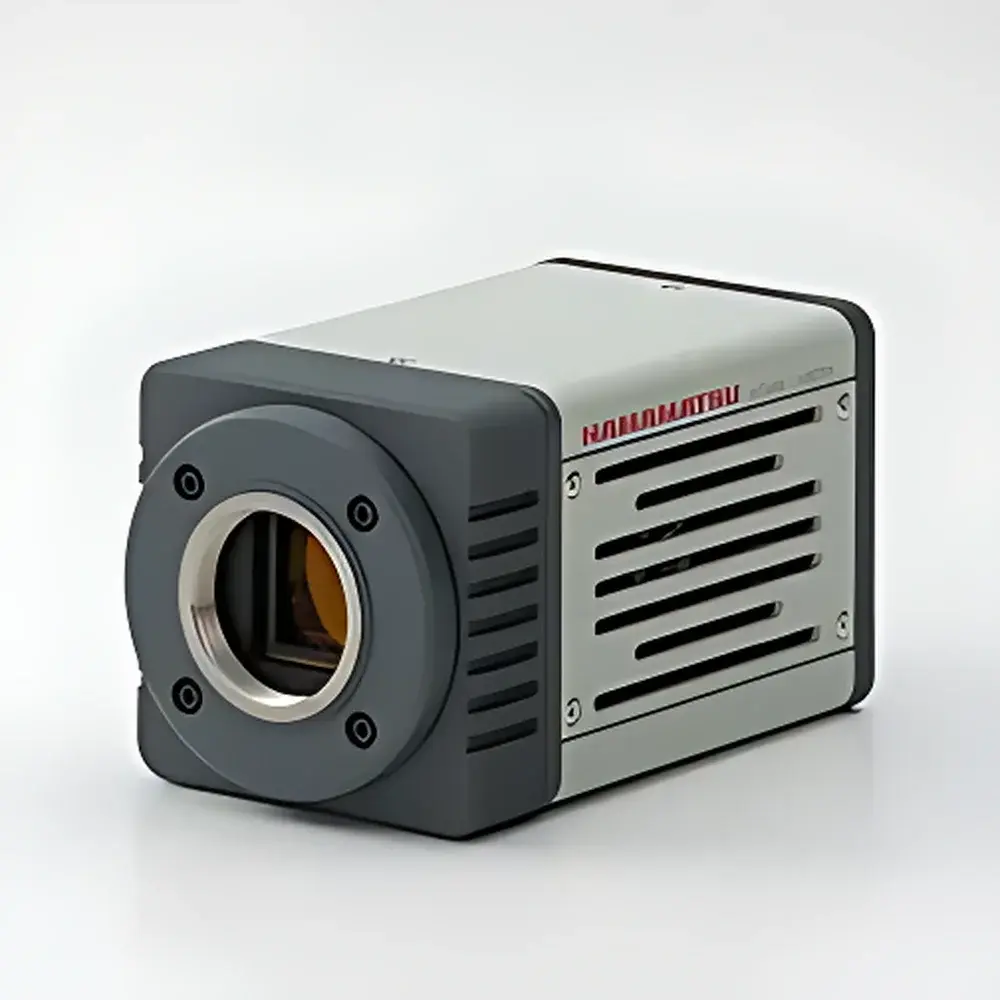
Hamamatsu C12741-03-02 InGaAs Near-Infrared Camera
| Brand | Hamamatsu |
|---|---|
| Origin | Japan |
| Manufacturer | Hamamatsu Photonics K.K. |
| Type | Imported OEM Instrument |
| Model | C12741-03-02 |
| Price Range | USD 13,500 – 68,000 (FOB Yokohama) |
| Resolution | 640 × 512 pixels |
| Active Area | 12.8 mm (H) × 10.24 mm (V) |
| Pixel Pitch | 20 µm (H) × 20 µm (V) |
| Cooling | Peltier-cooled to +10 °C (ambient +25 °C) |
| Frame Rate | 59.774 fps |
| Bit Depth | 14-bit digital output |
| Exposure Time | 16.7 ms – 1 s |
| Interface | USB 3.0 (Micro-B), SMA trigger input |
| Lens Mount | C-mount |
| Power Supply | DC +12 V, ~16 W |
| Operating Temperature | 0 °C to +40 °C |
| Humidity | 30–80% RH (non-condensing) |
Overview
The Hamamatsu C12741-03-02 is a high-performance, thermoelectrically cooled InGaAs (indium gallium arsenide) near-infrared (NIR) imaging camera engineered for quantitative scientific and industrial applications requiring spectral sensitivity from 950 nm to 1700 nm. Unlike silicon-based CCD or CMOS sensors—whose quantum efficiency drops sharply beyond 1100 nm—the C12741-03-02 leverages an optimized InGaAs photodiode array to deliver stable, low-noise responsivity across the short-wave infrared (SWIR) band. Its monolithic sensor architecture features integrated on-chip pixel-level uniformity correction, enabling reliable radiometric measurement without post-acquisition calibration drift. Designed for integration into automated optical inspection systems, laser diagnostics platforms, and materials characterization workflows, the camera operates at a stabilized sensor temperature of +10 °C via a two-stage Peltier cooler—ensuring thermal stability within ±0.5 °C under forced-air cooling at ambient +25 °C. This thermal control significantly suppresses dark current and fixed-pattern noise, supporting high-dynamic-range (HDR) imaging with reproducible linearity across exposure times from 16.7 ms to 1 s.
Key Features
- High quantum efficiency (>70% peak) in the 950–1700 nm spectral range, optimized for SWIR photon detection in semiconductor and photovoltaic analysis
- 640 × 512 pixel InGaAs focal plane array with 20 µm pitch, delivering 12.8 mm × 10.24 mm active imaging area and <0.37% defective pixel rate
- Peltier-based two-stage thermoelectric cooling system, maintaining sensor temperature at +10 °C (±0.5 °C) for low dark current (<100 e⁻/pixel/s) and high signal-to-noise ratio
- 14-bit digitization with hardware-level background subtraction and shading correction, minimizing spatial non-uniformity and enabling quantitative intensity mapping
- Real-time frame acquisition at 59.774 fps over USB 3.0 (USB 3.1 Gen 1 compliant), supporting synchronized multi-camera operation and time-resolved NIR imaging
- Flexible triggering architecture: edge-triggered, level-triggered, or start-triggered modes with programmable delay (0–1 s in 10 µs steps) via SMA input connector
- C-mount lens interface for compatibility with standard SWIR optics, including aspheric lenses, telecentric objectives, and bandpass filters (e.g., 1064 nm, 1310 nm, 1550 nm)
Sample Compatibility & Compliance
The C12741-03-02 is validated for non-destructive evaluation of optically opaque or semi-transparent materials where visible-light imaging fails. It enables direct visualization of subsurface structures in silicon wafers (e.g., crystal defects, dopant distribution, micro-cracks), MEMS device actuation, and solar cell junction integrity via carrier lifetime contrast. Its spectral response aligns with key industry standards: ASTM F2615-21 (for IR inspection of photovoltaic modules), ISO 10110-10 (optical element testing), and JEDEC JESD22-A113 (semiconductor package moisture ingress screening). The camera’s firmware supports audit-trail logging of acquisition parameters (exposure, gain, temperature, timestamp) required for GLP-compliant documentation. While not certified for medical or aerospace safety-critical use, its electrical design complies with IEC 61000-6-3 (EMC emission limits) and IEC 61010-1 (safety requirements for laboratory equipment).
Software & Data Management
Hamamatsu provides the proprietary HCImage Live software suite (Windows 10/11, 64-bit), offering real-time image display, histogram analysis, region-of-interest (ROI) statistics, and batch export in TIFF, HDF5, and CSV formats. The SDK (C/C++, Python, MATLAB APIs) supports custom integration into LabVIEW, Python-based automation frameworks (e.g., PyVISA, OpenCV), and industrial PLC-controlled inspection lines. All acquired images embed EXIF-style metadata—including sensor temperature, exposure duration, trigger mode, and firmware revision—ensuring traceability per FDA 21 CFR Part 11 requirements when used in regulated QA/QC environments. Background and flat-field correction matrices are stored in non-volatile memory and applied in real time; user-defined correction tables can be loaded externally for application-specific calibration.
Applications
- Semiconductor metrology: Inspection of silicon wafer backside defects, through-silicon via (TSV) alignment, and laser-induced thermal mapping during annealing
- Photovoltaic R&D: Quantitative assessment of minority carrier diffusion length in PERC, TOPCon, and tandem solar cells using luminescence imaging
- Laser beam profiling: Characterization of M² factor, beam centroid stability, and hot-spot detection for fiber lasers (1064 nm), telecom sources (1310/1550 nm), and ultrafast OPOs
- Food & agriculture: Non-contact moisture content mapping in grains, fruits, and leaf tissue based on 1450 nm and 1940 nm water absorption bands
- Cultural heritage science: Subsurface pigment layer analysis, underdrawing revelation in oil paintings, and parchment degradation monitoring
- Optical component testing: Coating uniformity verification on SWIR anti-reflection filters, lens barrel scatter analysis, and fiber coupling efficiency optimization
FAQ
Does the C12741-03-02 support external synchronization with other imaging or measurement instruments?
Yes—it features a dedicated SMA trigger input supporting edge-, level-, and start-trigger modes with sub-millisecond timing resolution and configurable delay (0–1 s in 10 µs increments), enabling precise temporal alignment with pulsed lasers, motion stages, or spectrometers.
What is the typical dark current performance at the specified operating temperature?
At +10 °C sensor temperature and 25 °C ambient, dark current is typically ≤100 electrons/pixel/second, measured at mid-range exposure (100 ms); this value remains stable over continuous operation exceeding 8 hours.
Can the camera be operated in vacuum or high-humidity environments?
No—the unit is rated for 30–80% RH (non-condensing) and standard atmospheric pressure only. Extended operation outside these conditions requires external environmental enclosure with controlled purge gas (e.g., dry N₂).
Is radiometric calibration available from Hamamatsu?
Hamamatsu provides factory-applied relative responsivity calibration (per-pixel gain/offset) and optional NIST-traceable absolute calibration (upon request, additional lead time and cost apply).
How is pixel non-uniformity corrected in real time?
The camera applies embedded, user-loadable correction matrices for both dark frame subtraction and flat-field shading correction—executed in hardware prior to ADC digitization, ensuring consistent linearity across the full dynamic range.


