Si-on-Ge Epitaxial Thin Film on N-Type Silicon Wafer
| Brand | 合肥科晶 |
|---|---|
| Origin | USA |
| Manufacturer Type | Authorized Distributor |
| Origin Category | Imported |
| Model | Si-on-Ge Epitaxial Thin Film |
| Price | Upon Request |
| Si Substrate | N-type, P-doped, Ø4″ × 0.5–0.55 mm, <100> orientation, 2 SEMI-standard flats, 0° off-axis, resistivity 1–10 Ω·cm, particle count <50 per wafer (≥0.20 µm) |
| Ge Epilayer | 0.5 µm ±3%, <100> orientation, N-type or P-type doping (1–5)×10¹⁹ cm⁻³ |
| Surface RMS Roughness | <2 nm |
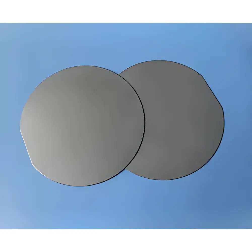
| Available Formats | Ø4″ wafers or 10×10 mm diced chips |
| Packaging | Vacuum-sealed Class 100 cleanroom bags in Class 1000 cleanroom environment, or individual cassette packaging |
Overview
The Si-on-Ge epitaxial thin film is a high-purity, single-crystal heterostructure engineered for advanced semiconductor research and device prototyping. This product consists of a precisely controlled germanium (Ge) epilayer grown via ultra-high-vacuum chemical vapor deposition (UHV-CVD) or molecular beam epitaxy (MBE) onto a polished N-type silicon (Si) substrate. The lattice-mismatched Si/Ge interface is stabilized through graded buffer layers or low-temperature nucleation techniques to minimize threading dislocation density—critical for optoelectronic, photodetector, and strained-silicon CMOS applications. Unlike polycrystalline or sputtered Ge films, this epitaxial structure delivers long-range crystalline coherence, enabling carrier mobility enhancement, reduced interface trap density, and reproducible band alignment characterization. It serves as a foundational platform for heterojunction bipolar transistors (HBTs), mid-infrared photonics, and silicon photonics integration where monolithic compatibility with CMOS fabrication infrastructure is essential.
Key Features
- Atomically smooth Ge surface with root-mean-square (RMS) roughness <2 nm, verified by atomic force microscopy (AFM) and confirmed across full 4-inch wafers
- Controlled Ge layer thickness of 0.5 µm ±3%, measured in-line using high-resolution X-ray reflectivity (XRR) and cross-sectional transmission electron microscopy (XTEM)
- Single-crystal orientation maintained in both Si substrate and Ge epilayer, ensuring consistent anisotropic transport properties
- Doping flexibility: configurable N-type (e.g., As or Sb) or P-type (e.g., B) activation at (1–5)×10¹⁹ cm⁻³, validated by Hall effect and secondary ion mass spectrometry (SIMS)
- Substrate compliance: SEMI-standard 4-inch N-type Si wafers with two flats, orientation, 0° off-axis, resistivity 1–10 Ω·cm, and ≤50 particles ≥0.20 µm per wafer
- Trace contamination control: heavy metal impurities (Fe, Cu, Ni) <1×10¹⁰ cm⁻², certified via total reflection X-ray fluorescence (TXRF)
Sample Compatibility & Compliance
This Si-on-Ge epitaxial film is fully compatible with standard semiconductor cleanroom processes—including photolithography, dry etching (ICP-RIE), thermal oxidation, and metal sputtering—without delamination or interfacial degradation. All wafers undergo rigorous pre-shipment inspection per SEMI MF1530 (Particle Counting) and SEMI MF1390 (Surface Flatness). The material meets baseline requirements for ISO 14644-1 Class 5 (Class 100) cleanroom handling and is packaged under inert gas (N₂ or Ar) in vacuum-sealed, static-dissipative Class 100 cleanroom bags. While not certified to specific FDA or IEC standards (as it is a research-grade substrate, not a finished medical or safety-critical device), its fabrication documentation supports GLP-compliant lab records and traceability for academic, government, and industrial R&D reporting frameworks.
Software & Data Management
No embedded firmware or proprietary software is associated with this passive epitaxial substrate. However, comprehensive metrology data—including XRR thickness profiles, SIMS dopant depth profiles, AFM topography maps, and XRD ω-2θ scans—is provided digitally upon request in standardized formats (CSV, TIFF, .xye) for integration into institutional LIMS or data analysis pipelines (e.g., Python-based SciPy/Matplotlib, MATLAB, or commercial tools like Igor Pro). Batch-specific certificates of conformance include lot number, growth date, inspection timestamps, and operator ID—enabling full audit trail alignment with ISO/IEC 17025 laboratory accreditation practices.
Applications
- Strained-Si channel engineering for high-mobility MOSFETs and FinFETs
- Heterostructure photodetectors operating in the 1.3–1.55 µm telecom wavelength range
- Ge-on-Si waveguide platforms for integrated silicon photonics
- Model system for studying dislocation dynamics and strain relaxation mechanisms in lattice-mismatched heteroepitaxy
- Seed layer for subsequent III-V compound semiconductor growth (e.g., GaAs, InGaAs) via direct wafer bonding
- Calibration reference for Raman spectroscopy intensity mapping and strain quantification protocols
FAQ
Is this Ge layer fully relaxed or pseudomorphic?
The 0.5 µm Ge epilayer exhibits partial relaxation (~70–85% strain relief) depending on growth conditions; full relaxation is achievable with thicker layers (>1.5 µm) or annealing. XRD rocking curve FWHM and Raman peak shift analysis are recommended to quantify residual strain.
Can these wafers be used for direct e-beam lithography?
Yes—low surface roughness and absence of conductive coating make them suitable for high-resolution e-beam patterning; optional conductive anti-charging treatment (e.g., 5 nm Cr or Au) can be applied upon request.
What is the typical threading dislocation density (TDD)?
Measured TDD ranges from 1×10⁶ to 5×10⁷ cm⁻², depending on buffer architecture; TEM cross-section reports are available for qualified lots.
Do you offer custom doping profiles (e.g., delta-doping or gradient doping)?
Yes—custom MBE or CVD runs with tailored dopant incorporation sequences are available under NDA for qualified research partners.
Are diced 10×10 mm chips cleaved or saw-cut?
All diced chips are precision diamond-blade saw-cut with edge chipping <1 µm and post-cut plasma cleaning to remove debris and native oxide residues.