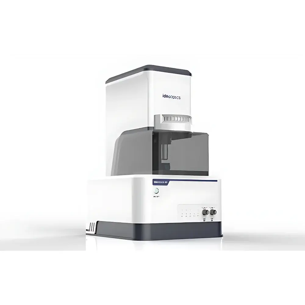
IdeaOptics QFLSVision™ Quasi-Fermi-Level Splitting Imaging System
| Brand | IdeaOptics |
|---|---|
| Origin | Shanghai, China |
| Manufacturer | Yes |
| Country of Origin | China |
| Model | QFLSVision™ |
| Pricing | Upon Request |
| Spatial Resolution | 1 µm |
| Capabilities | Photoluminescence (PL) Intensity & Peak Position Mapping, PL Quantum Yield (PLQY) & QFLS Mapping, Pseudo j–V Curve Reconstruction, Non-Device-State Optical PCE Estimation, Dual-Excitation Channel Support |
Overview
The IdeaOptics QFLSVision™ Quasi-Fermi-Level Splitting Imaging System is a high-precision optical metrology platform engineered for quantitative, spatially resolved characterization of thin-film photovoltaic materials—particularly perovskite solar cells (PSCs). It operates on the physical principle of photoluminescence-based quasi-Fermi-level splitting (QFLS) quantification, where the energy separation between electron and hole quasi-Fermi levels is derived from calibrated electroluminescence (EL) or photoluminescence (PL) spectra under controlled excitation. Unlike conventional intensity-only imaging, QFLSVision™ integrates absolute spectral radiance calibration, temperature-stabilized detection, and physics-informed algorithms to convert spectral data into quantitative QFLS maps with sub-micrometer spatial resolution (≤1 µm). This enables direct correlation between local optoelectronic properties—such as radiative recombination efficiency, defect-mediated non-radiative losses, and interfacial carrier dynamics—and material microstructure, without requiring full device fabrication.
Key Features
- Quantitative QFLS Mapping: Delivers pixel-resolved QFLS values (in eV) derived from spectrally resolved PL/EL emission, traceable to NIST-traceable irradiance standards via in-situ calibration routines.
- Dual-Excitation Architecture: Supports two independently tunable excitation wavelengths (e.g., 405 nm and 532 nm), enabling selective probing of different perovskite compositions, band alignments in tandem stacks, and depth-dependent carrier generation profiles.
- Sub-Second Multidimensional Acquisition: Simultaneously captures spatial, spectral (200–1000 nm), and intensity dimensions at frame rates up to 1 Hz for full-field mapping—enabling kinetic studies under variable illumination or bias conditions.
- Non-Device-State Characterization: Performs layer-by-layer QFLS assessment on films, pre-contact layers, and semi-fabricated devices—providing early-stage feedback on bulk recombination, interfacial trap density, and phase segregation prior to metallization.
- Integrated Electrical Interface: Compatible with external source-measure units (SMUs) via standardized BNC and SMA ports; supports synchronized voltage/current biasing during optical acquisition for carrier transport loss analysis under operating conditions.
- Pseudo j–V & Optical PCE Prediction: Reconstructs spatially resolved pseudo current–voltage curves and estimates maximum theoretical power conversion efficiency (PCE) from QFLS and PLQY maps—without electrical contacts or encapsulation.
Sample Compatibility & Compliance
QFLSVision™ accommodates standard photovoltaic substrates (glass, ITO, FTO, NiOx, SnO2) and film thicknesses ranging from 1 µm. It supports ambient, inert-gas, and low-humidity (<5% RH) environments via optional glovebox integration. The system adheres to ISO/IEC 17025 principles for measurement uncertainty reporting and includes built-in audit trails for calibration history, exposure settings, and algorithm versioning—supporting GLP-compliant R&D workflows. While not a regulatory instrument per se, its output parameters align with ASTM E3086–22 (Standard Guide for Photoluminescence Characterization of Perovskite Photovoltaic Materials) and inform USP analytical instrument qualification protocols.
Software & Data Management
The QFLSVision™ Control Suite is a Windows-based application supporting real-time spectral visualization, batch processing of hyperspectral cubes, and export of calibrated data in HDF5 and TIFF formats with embedded metadata (wavelength grid, irradiance calibration coefficients, temperature logs). All processing pipelines—including PLQY correction, QFLS calculation, peak fitting, and PCE estimation—are scriptable via Python API (PyQFLS), enabling integration into automated analysis workflows. Audit logs record user actions, parameter changes, and software versioning in accordance with FDA 21 CFR Part 11 requirements for electronic records and signatures. Raw spectral data retains full bit-depth (16-bit) and wavelength fidelity for third-party validation.
Applications
- Recombination Loss Profiling: Differentiates bulk Shockley–Read–Hall (SRH) recombination from interface-assisted losses by correlating QFLS gradients with cross-sectional SEM/EDS data.
- Film Uniformity Assessment: Maps PL peak position shifts (±0.5 nm sensitivity) to identify chemical inhomogeneity (e.g., halide segregation) and strain-induced bandgap variations across large-area coatings.
- Tandem Cell Optimization: Evaluates interlayer energy alignment and current-matching constraints in perovskite/silicon and all-perovskite stacks using dual-excitation QFLS contrast.
- Process Development Feedback: Quantifies impact of annealing temperature, anti-solvent treatment, or passivation layers on local QFLS distribution—accelerating DOE-driven optimization cycles.
- Stability Mechanism Studies: Tracks QFLS decay kinetics under thermal stress, UV exposure, or humidity ingress to isolate degradation pathways at sub-micron scale.
FAQ
What does QFLS physically represent in perovskite solar cells?
QFLS reflects the maximum achievable open-circuit voltage (VOC) under given illumination and temperature conditions—it is directly proportional to the difference between electron and hole quasi-Fermi levels, governed by the detailed balance of radiative and non-radiative recombination.
Can QFLSVision™ measure QFLS on opaque or metal-backed samples?
Yes—via front-side EL or transmission-mode PL on semi-transparent electrodes; for fully opaque stacks, top-emission geometry with optimized collection optics ensures signal capture without substrate interference.
Is spectral calibration performed in situ or requires external reference sources?
The system includes an integrated, thermally stabilized NIST-traceable irradiance standard lamp and automated shutter sequence for daily in-situ calibration—no external hardware required for routine operation.
How is PLQY quantified without integrating spheres?
Using a calibrated reference sample method combined with absolute radiance calibration and solid-angle correction, achieving ±3% relative uncertainty across the visible-NIR range (400–950 nm).
Does the software support batch processing of multi-sample datasets?
Yes—the Batch Processor module enables parallel analysis of hundreds of hyperspectral cubes with user-defined ROI masks, normalization schemes, and statistical aggregation (mean, std, min/max per pixel).


