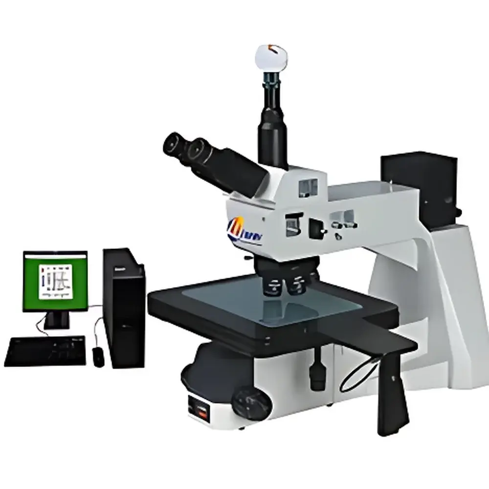
YANRUN 8XB-PC Large-Platform Inverted Metallurgical Microscope for Semiconductor Chip Inspection
| Brand | YANRUN |
|---|---|
| Origin | Shanghai, China |
| Manufacturer Type | Direct Manufacturer |
| Origin Category | Domestic (China) |
| Model | 8XB-PC |
| Configuration | Inverted |
| Eyepieces | WF10× (25 mm FOV), WF10× (20 mm FOV) with 0.1 mm crosshair reticle |
| Objectives | 5×/0.1 BD (W.D. 29.4 mm), 10×/0.25 BD (W.D. 16 mm), 20×/0.40 BD (W.D. 10.6 mm), 40×/0.60 BD (W.D. 5.4 mm) |
| Stage | Dual-layer mechanical stage (350 × 310 mm, travel range 250 × 250 mm) |
| Illumination | Reflected Köhler illumination with adjustable 12 V / 100 W halogen lamp, aperture & field diaphragms |
| Focus Mechanism | Coaxial coarse/fine focusing, rack-and-pinion drive, fine focus graduation: 2 µm |
| Polarization System | Rotatable analyzer (0–360°), removable polarizer and analyzer |
| Filters | Insert-type blue, green, neutral density |
| Accessories Included | 0.01 mm stage micrometer, 0.5× C-mount adapter, USB digital camera (basic resolution), polarizing kit, filter set, documentation set |
| Optional | Long-working-distance BD objectives (50×, 80×, 100×), high-resolution digital cameras (2–12 MP), DIC modules (10×, 20×, 40×, 100×), research-grade image analysis software, C-mount adapters for DSLR/mirrorless systems |
Overview
The YANRUN 8XB-PC is an inverted metallurgical microscope engineered specifically for high-precision inspection of semiconductor wafers, packaged ICs, bond pads, solder bumps, and failure analysis (FA) samples in microelectronics manufacturing and R&D laboratories. Its inverted optical configuration places the objective lenses beneath the specimen stage—enabling unobstructed access to large, heavy, or top-mounted fixtures such as probe stations, thermal chucks, or vacuum clamps. The system utilizes an infinity-corrected, plan-apochromatic optical path optimized for brightfield (BF), darkfield (DF), and polarized light (POL) contrast modes. All standard objectives are strain-free, semi-apochromatic, and designed for reflected-light illumination with built-in beam-splitting capability to support future DIC or fluorescence upgrades. The microscope conforms to ISO 10934-1 (microscopy — nomenclature and terminology) and meets essential mechanical stability requirements defined in ASTM E2015 for metallurgical microscopes used in quality control environments.
Key Features
- Inverted platform architecture with reinforced base and vibration-damped column, supporting stable imaging of substrates up to 300 mm in diameter and weighing over 5 kg.
- Large-format mechanical stage (350 × 310 mm footprint, 250 × 250 mm travel range) accommodates full-wafer carriers, PCB panels, and multi-chip modules without repositioning.
- Five-position objective turret with dedicated DIC slots—compatible with optional Nomarski differential interference contrast modules for sub-micron topographic contrast enhancement.
- Reflected Köhler illumination system featuring a 12 V / 100 W halogen source with continuously variable intensity control (AC 85–230 V input), precision aperture and field diaphragms, and integrated heat-absorbing glass to minimize thermal drift during extended observation.
- Coaxial coarse/fine focusing mechanism with dual-scale vernier readout; fine focus calibrated to 2 µm per division, ensuring repeatable Z-axis positioning for layer-by-layer inspection and focus stacking workflows.
- Full polarization suite: rotatable analyzer (0–360° graduated scale), removable polarizer and analyzer, enabling quantitative birefringence assessment of dielectric layers, stress-induced anisotropy in SiN passivation, or crystal orientation mapping.
Sample Compatibility & Compliance
The 8XB-PC supports a broad range of non-transmissive specimens typical in semiconductor process control: silicon wafers (bare and patterned), ceramic substrates, metal interconnects, power device dies, MEMS structures, and encapsulated packages. Its long working distance objectives (minimum W.D. = 5.4 mm at 40×) permit clearance for probe needles, thermal sensors, or environmental chambers mounted above the sample. The stage accepts standard SEM-style stubs, vacuum chucks (via M6 threaded holes), and custom fixtures. The system complies with CE safety directives (2014/35/EU Low Voltage Directive and 2012/19/EU EMC Directive) and satisfies mechanical robustness benchmarks referenced in ISO 9001-certified QA labs. While not FDA 21 CFR Part 11–validated out-of-the-box, its hardware architecture allows integration with compliant image management platforms when paired with validated third-party software.
Software & Data Management
The base configuration includes a standard USB 2.0 digital camera and 0.5× C-mount adapter, delivering real-time preview and static capture at VGA resolution. Raw image data is saved in TIFF or BMP format with embedded metadata (objective magnification, exposure time, timestamp). Optional high-resolution cameras (2–12 MP) support lossless RAW capture and hardware-triggered acquisition synchronized with external equipment (e.g., probe station controllers). When upgraded with YANRUN’s optional ImagePro Insight or open-source alternatives (e.g., Fiji/ImageJ), the system enables particle counting, line profile analysis, grain size quantification per ASTM E112, and automated defect classification via threshold-based segmentation. Audit trails, user access logs, and calibration history can be maintained externally under GLP/GMP-aligned documentation protocols.
Applications
- Wafer-level defect review: identification of scratches, particles, residue, delamination, and etch non-uniformity on front-side metallization.
- Package integrity inspection: wire bond loop geometry, solder joint wetting angle, mold compound voids, and lid seal verification.
- Failure analysis: cross-section evaluation of via structures, trench isolation, gate oxide integrity, and electromigration damage sites.
- Material characterization: grain structure analysis in copper redistribution layers (RDL), recrystallization mapping after annealing, and stress-induced birefringence in low-k dielectrics.
- Process validation: monitoring CMP endpoint uniformity, lithography alignment accuracy, and plating thickness consistency via comparative reflectance contrast.
FAQ
Is the 8XB-PC compatible with automated stage controllers or motorized focus units?
Yes—standard RS-232 and USB TTL interfaces are预留 for OEM integration; third-party motorized stages (e.g., Prior, Ludl) and focus drives can be added via optional controller modules.
Can this microscope be used for quantitative metallography per ASTM E112 or ISO 643?
With optional high-resolution camera and certified image analysis software, yes—the system supports grain size measurement using intercept and planimetric methods, provided calibration is performed using NIST-traceable stage micrometers.
Does the halogen illumination support color-critical applications such as thin-film interference analysis?
The 12 V / 100 W halogen source provides stable CCT (~3200 K) and sufficient spectral continuity from 400–1000 nm; however, for precise film-thickness metrology, users should supplement with monochromatic LED sources or spectrally calibrated white-light interferometers.
What is the maximum sample height clearance under the objectives?
At 5× magnification (longest W.D.), vertical clearance is 29.4 mm; at 40×, it reduces to 5.4 mm—sufficient for most wafer carriers and test sockets, but insufficient for tall TO-can packages without stage lowering.
Are replacement bulbs and fuses supplied with the instrument?
One spare 12 V / 100 W halogen bulb and two 4 A slow-blow fuses are included in the standard accessory kit; additional consumables are available through YANRUN’s authorized service network in APAC and EU regions.


