HORIBA HCLUE High-Resolution Cathodoluminescence Spectroscopy System
| Brand | HORIBA |
|---|---|
| Origin | France |
| Manufacturer Type | Authorized Distributor |
| Import Status | Imported |
| Model | HCLUE |
| Pricing | Available Upon Request |
Overview
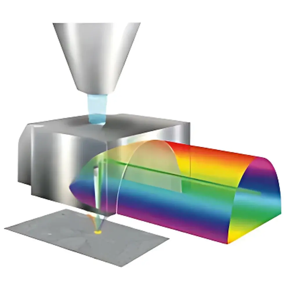
The HORIBA HCLUE is a high-resolution cathodoluminescence (CL) spectroscopy system engineered for integration with scanning electron microscopes (SEM) and transmission electron microscopes (TEM). It operates on the fundamental principle of cathodoluminescence: when a focused electron beam impinges on a solid-state sample, electron-hole pairs are generated; their recombination emits photons whose energy distribution reflects the material’s electronic band structure, defect states, dopant configuration, and local crystallographic environment. Unlike conventional photoluminescence or electroluminescence techniques, CL provides nanoscale spatial correlation between structural morphology (imaged in real time via SEM/TEM) and spectral emission—enabling quantitative, position-resolved optical characterization at sub-100 nm resolution. The HCLUE system is built upon HORIBA’s legacy in precision optical instrumentation and leverages optimized mirror-coupled light collection to maximize photon throughput from the specimen chamber, minimizing signal loss inherent in fiber-based or lens-coupled alternatives.
Key Features
- Mirror-coupled optical interface: Direct parabolic mirror collection ensures >65% light collection efficiency across UV–NIR range without chromatic aberration or alignment drift.
- Modular spectrograph architecture: Compatible with iHR series spectrometers (320 mm, 550 mm focal lengths), enabling selection of spectral resolution (down to 0.08 nm @ 500 nm with 2400 g/mm grating) versus throughput trade-offs.
- Dual-detector capability: Simultaneous mounting of back-illuminated CCD (185–1100 nm) and InGaAs array (900–2500 nm) extends full spectral coverage to 185–2500 nm without mechanical reconfiguration.
- Multi-modal acquisition: Supports point-spectrum acquisition, line scans (1D spectral profiles), and hyperspectral mapping (2D CL imaging with full spectrum per pixel).
- SWIFT™ fast mapping mode: Synchronizes beam scanning with detector readout for frame rates up to 30 fps at 256 × 256 pixel resolution, compatible with standard SEM scan generators.
- Vacuum-compatible design: All optical components rated for ≤10⁻⁵ mbar operating pressure; no internal O-rings or adhesives that outgas under electron-beam exposure.
Sample Compatibility & Compliance
The HCLUE system accommodates bulk solids, thin films, nanowires, quantum dots, and geological thin sections—provided samples are conductive or coated with ≤5 nm carbon or Au/Pd. Non-conductive specimens require charge compensation via low-kV operation (<5 kV) or beam deceleration. The system complies with IEC 61000-6-3 (EMC emissions) and IEC 61000-6-2 (immunity), and its software architecture supports audit trails, user access levels, and electronic signatures required for GLP and GMP environments. While CL itself is not governed by a single ISO standard, data acquisition protocols align with ASTM E2715–22 (Standard Guide for Cathodoluminescence Analysis of Inorganic Materials) and ISO/IEC 17025:2017 clause 7.7 (traceability of measurement results).
Software & Data Management
Control and analysis are performed using HORIBA’s LabSpec 6 platform, a modular suite certified for FDA 21 CFR Part 11 compliance (with optional 21 CFR Part 11 module enabled). The software supports real-time spectral preview during acquisition, batch processing of hyperspectral cubes (e.g., PCA, MCR-ALS unmixing), peak fitting (Voigt, Gaussian models), and export to HDF5, TIFF, or ASCII formats for third-party tools (Python, MATLAB, HyperSpy). Raw spectra include embedded metadata: beam energy, working distance, dwell time, grating position, detector temperature, and spectrometer calibration coefficients—all traceable to NIST-traceable wavelength standards.
Applications
- Semiconductors & optoelectronics: Mapping dislocation-related non-radiative recombination in GaN LEDs, identifying SiC polytype boundaries, quantifying AlGaN alloy composition gradients via band-edge shift.
- Geosciences & mineralogy: Distinguishing zircon metamictization stages via CL intensity decay kinetics; differentiating dolomite from calcite using Mn²⁺/Fe²⁺ emission ratios (580 nm vs. 700 nm); detecting trace REE incorporation in apatite.
- Dielectrics & oxides: Characterizing oxygen vacancy distributions in HfO₂ gate dielectrics; correlating Ti³⁺ luminescence (420 nm) with resistive switching filaments in memristor stacks.
- Life sciences (ex vivo):strong> Imaging biomineralization in bone cross-sections (hydroxyapatite CL at 420 nm) and dental enamel defects using low-dose CL-SEM.
- Forensics: Discriminating synthetic vs. natural diamond origin via nitrogen-aggregate CL signatures (H3 center at 503.2 nm, ND1 at 415 nm), and identifying pigment degradation products in historical paint layers.
FAQ
What vacuum compatibility does the HCLUE system require?
The optical coupling module operates continuously at SEM chamber pressures ≤10⁻⁵ mbar; no additional differential pumping is needed.
Can the HCLUE be retrofitted onto existing SEM platforms?
Yes—it supports standard SEM flange interfaces (CF100, CF160) and integrates with Thermo Fisher, Zeiss, JEOL, and Hitachi SEM control buses via TTL/RS-232 or Ethernet APIs.
Is spectral calibration traceable to national standards?
All spectrometers ship with NIST-traceable Hg/Ar/Ne lamp calibration certificates; in situ recalibration is supported using integrated LED reference sources.
How is spatial resolution defined in CL mapping?
Effective resolution is determined by electron beam spot size, carrier diffusion length, and optical collection geometry—typically 10–50 nm for direct-bandgap semiconductors, up to 200 nm for wide-bandgap insulators.
Does HORIBA provide application-specific method templates?
Yes—pre-configured workflows for GaN defect analysis, zircon geochronology, and diamond provenance screening are included in LabSpec 6 and updated quarterly via HORIBA’s Application Support Portal.