MicroChem gL2000 Electron-Beam Negative Tone Photoresist Series
| Brand | MicroChem Corp |
|---|---|
| Origin | USA |
| Product Variants | gL2000-L, gL2000-M, gL2000-H |
| Developer Options | gL Developer, gL Developer HR |
| Rinse Agent | gL Rinse |
| Stripper | gL Remover |
| Etch Resistance | Superior to PMMA |
| Resolution Capability | Sub-10 nm (under optimized e-beam conditions) |
| Tone | Negative |
| Processing | Aqueous-based development |
Overview
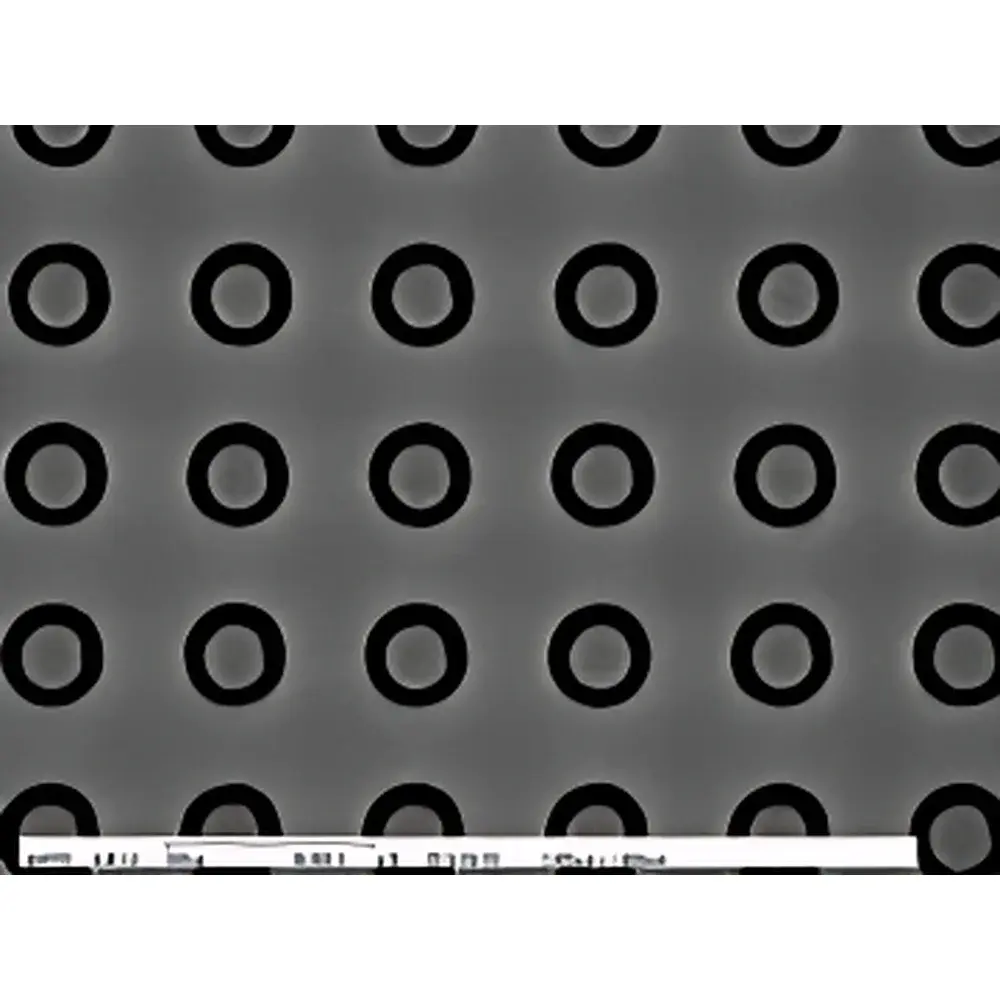
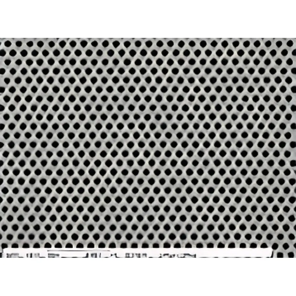
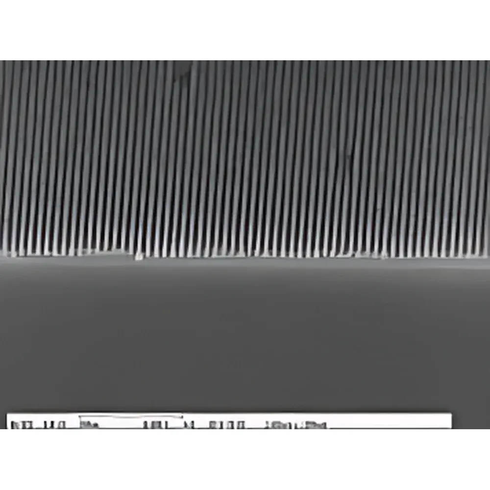
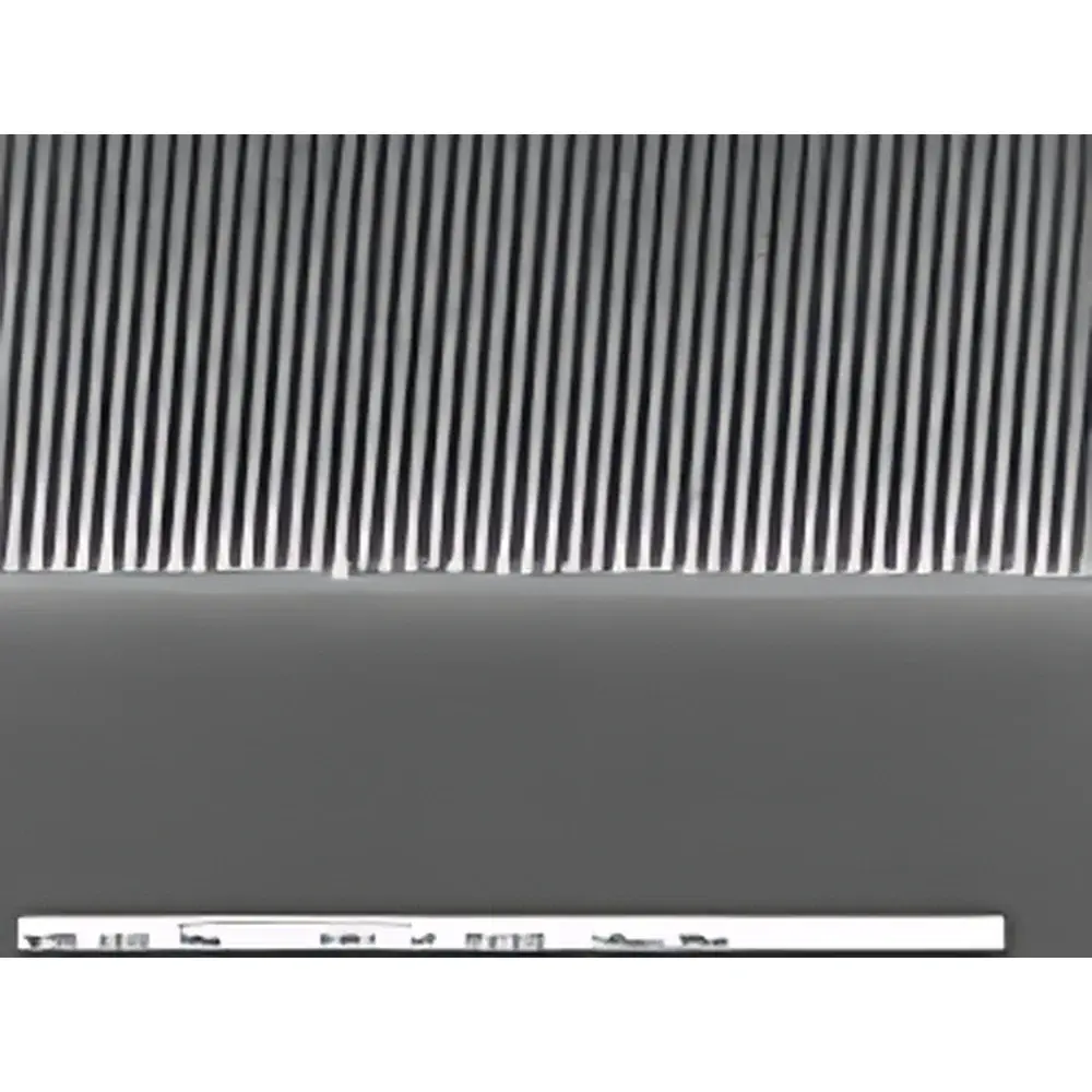
The MicroChem gL2000 series is a high-performance, chemically amplified negative-tone electron-beam (e-beam) resist engineered for advanced nanofabrication in semiconductor R&D, mask making, and quantum device prototyping. Unlike conventional polymethyl methacrylate (PMMA), the gL2000 resists employ a proprietary polyhydroxystyrene (PHS)-based matrix with acid-labile protecting groups, enabling high sensitivity (≤ 10 µC/cm² at 100 keV), excellent contrast (γ > 5), and sub-10 nm resolution under optimized exposure and development protocols. Its negative-tone behavior arises from acid-catalyzed crosslinking during post-exposure bake (PEB), rendering exposed regions insoluble in aqueous alkaline developers. The system is fully compatible with standard e-beam lithography platforms—including Raith, JEOL, and Zeiss systems—and integrates seamlessly into cleanroom workflows requiring high throughput and process reproducibility.
Key Features
- Three calibrated sensitivity grades: gL2000-L (low-sensitivity, high-resolution stability), gL2000-M (balanced sensitivity/resolution), and gL2000-H (high-sensitivity, rapid throughput)
- Aqueous developable—eliminates need for organic solvents and reduces environmental and safety compliance burden
- Superior dry etch resistance versus PMMA, with demonstrated selectivity >3:1 in Cl₂/O₂ and SF₆ plasma etches for Si, SiO₂, and metal hard masks
- Controlled dissolution kinetics enabling tunable line-edge roughness (LER) < 2.5 nm RMS via developer concentration, temperature, and time modulation
- Thermal stability up to 180 °C pre-bake and 130 °C PEB—compatible with multilayer resist schemes and lift-off processes
- Spin-coatable from standard anisole or PGMEA solutions; film uniformity < ±2% across 100 mm wafers
Sample Compatibility & Compliance
The gL2000 series is validated on silicon, fused silica, SiNₓ, and metal substrates (Au, Cr, Ti). It meets ASTM E1941–22 guidelines for resist characterization and is routinely employed in facilities operating under ISO/IEC 17025-accredited quality management systems. While not classified as a medical device or FDA-regulated product, its manufacturing adheres to MicroChem’s internal Good Manufacturing Practice (GMP)-aligned controls, including lot traceability, Certificate of Analysis (CoA), and rigorous QC testing for viscosity, solids content, and shelf-life stability (24 months refrigerated at 2–8 °C). The resist formulation contains no SVHCs listed under EU REACH Annex XIV and complies with RoHS Directive 2011/65/EU.
Software & Data Management
gL2000 does not incorporate embedded firmware or proprietary control software. Instead, it operates within established e-beam lithography environments (e.g., Nanometer Pattern Generation System (NPGS), JBX Control Center, or Elphy Quantum). Process data—including dose calibration curves, contrast curves (log-log plots), and development rate integrals—is generated using industry-standard metrology tools (CD-SEM, AFM, optical scatterometry) and stored in vendor-neutral formats (CSV, TIFF, GDSII). Full audit trails for resist lot usage, bake parameters, and development conditions are maintained per GLP/GMP-aligned lab documentation practices. For regulatory submissions, gL2000 supports 21 CFR Part 11-compliant electronic records when integrated with validated LIMS or ELN platforms.
Applications
- Fabrication of sub-20 nm gate structures and finFET test patterns in academic and industrial CMOS research
- Maskless direct-write lithography for photomask repair and custom reticle prototyping
- Nanopatterning of plasmonic metasurfaces, superconducting qubit architectures, and 2D material heterostructures
- High-aspect-ratio nanoimprint stamp fabrication requiring deep etch resilience
- Multi-level alignment stacks where thermal budget and interlayer compatibility are critical
FAQ
What is the recommended spin speed range for achieving 100–300 nm gL2000 films?
Typical spin speeds range from 2,500 to 6,000 rpm depending on solvent choice and target thickness; precise calibration curves are provided in the Technical Data Sheet for each variant.
Can gL2000 be used with UV or DUV exposure sources?
No—it is specifically formulated for electron-beam exposure and lacks photosensitivity to UV/DUV wavelengths; using non-e-beam sources results in negligible latent image formation.
Is gL Developer HR compatible with standard wafer track systems?
Yes—its low volatility and aqueous composition enable integration with semi-automated and fully automated track platforms equipped for TMAH-based developers.
How should expired gL2000 resist be disposed?
Expired material must be treated as hazardous chemical waste per local EPA or equivalent regulatory authority requirements; never pour down drains or discard in general waste.
Does MicroChem provide dose calibration services?
MicroChem supplies comprehensive dose-response datasets for each lot; end-user calibration using on-site CD-SEM metrology is required for process transfer and tool matching.
Related Products


