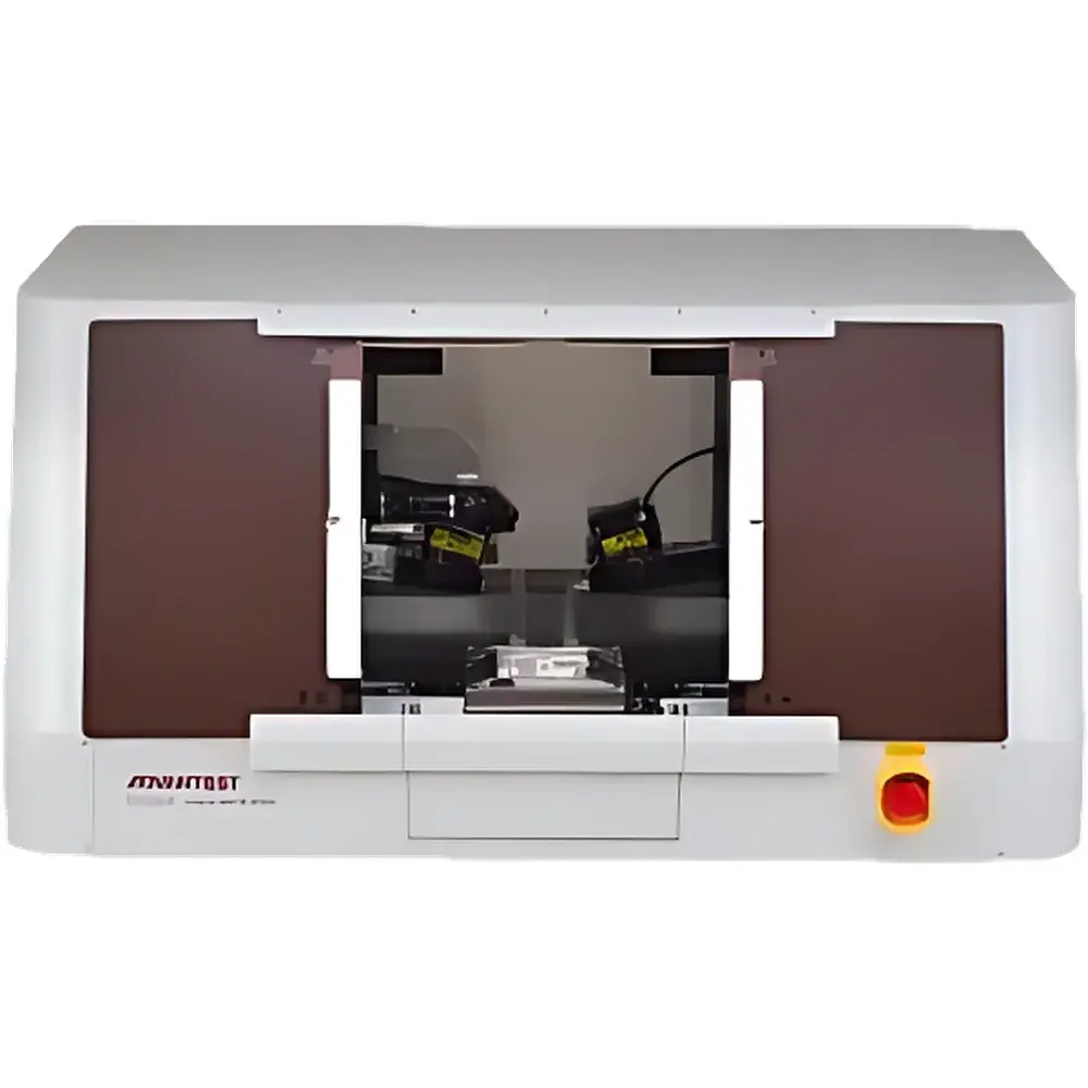
Advantest TS9000 High-Resolution Time-Domain Reflectometer (TDR) and Time-Domain Transmissometer (TDT) System
| Brand | Advantest |
|---|---|
| Origin | Japan |
| Model | TS9000 |
| Type | TDR/TDT Integrated Measurement System |
| Application Domain | Non-destructive Fault Localization in IC Packages and PCB Interconnects |
| Compliance Context | Supports JEDEC JESD22-B111, IPC-TM-650 2.5.1, and IEEE Std 1149.1 (JTAG) auxiliary diagnostics |
Overview
The Advantest TS9000 is a high-resolution, integrated time-domain reflectometry (TDR) and time-domain transmissometry (TDT) measurement system engineered for non-destructive fault localization in advanced semiconductor packaging and printed circuit board (PCB) interconnect structures. Leveraging proprietary terahertz-range ultra-short electrical pulse generation—derived from Advantest’s established THz signal analysis platform—the TS9000 delivers sub-millimeter spatial resolution in impedance profiling. Unlike conventional nanosecond-scale TDR instruments, the TS9000 employs picosecond-duration excitation pulses with bandwidth exceeding 100 GHz, enabling precise discrimination of impedance discontinuities arising from microstructural defects such as open vias, solder joint voids, trace delamination, or TSV (through-silicon via) contact failures. The system operates on the fundamental principle of launching a known fast-rising step or impulse into a transmission line and analyzing the amplitude, polarity, and time-of-flight of reflected (TDR) or transmitted (TDT) signals to infer impedance variations along the path. This enables quantitative mapping of characteristic impedance (Z₀), reflection coefficient (Γ), and propagation delay—critical parameters for signal integrity validation in high-speed digital and RF packaging.
Key Features
- Integrated dual-mode architecture supporting both TDR (reflection-based) and TDT (transmission-based) measurements on a single platform
- Picosecond-class pulse generator with <15 ps rise time and >100 GHz effective bandwidth for sub-50 µm spatial resolution
- Real-time waveform acquisition at up to 200 GS/s sampling rate with 12-bit vertical resolution
- Automated fault signature classification engine identifying opens, shorts, stubs, impedance mismatches, and distributed losses
- CAD-overlay visualization module aligning measured time-domain responses with native Gerber or ODB++ layout data for precise physical coordinate mapping
- Probe-compatible interface supporting both coaxial SMPM and microwave wafer-probe configurations for package-level and die-level access
- Thermal drift-compensated calibration suite compliant with ISO/IEC 17025 traceability requirements
Sample Compatibility & Compliance
The TS9000 is validated for characterization of heterogeneous interconnect structures including flip-chip microbumps (Cu-pillar, solder, and polymer-underfill interfaces), 2.5D/3D stacked packages with silicon interposers, organic substrates (ABF, BT), and high-density PCBs with embedded passives. It supports non-contact probing via high-frequency microwave probes and direct contact using calibrated launch fixtures. The system meets metrological requirements outlined in JEDEC JESD22-B111 (Board-Level Drop Test Correlation), IPC-TM-650 Section 2.5.1 (TDR Impedance Measurement), and IEEE Std 1149.1 Annex D (Boundary-Scan Assisted Structural Test). Data audit trails and user-access controls are configurable to support GLP/GMP environments under FDA 21 CFR Part 11 compliance frameworks.
Software & Data Management
The TS9000 is operated via Advantest’s proprietary TDRView™ software suite, which provides full waveform editing, differential impedance extraction, S-parameter conversion (via time-to-frequency domain transformation), and statistical process control (SPC) charting. All measurement sessions generate timestamped, digitally signed binary archives (.tdrbin) containing raw waveforms, calibration metadata, probe compensation settings, and CAD alignment parameters. Export options include CSV, HDF5, and Touchstone (S2P) formats. Role-based access control (RBAC), electronic signatures, and revision-controlled report templates ensure alignment with regulated quality management systems.
Applications
- Root-cause analysis of C4/microbump opens and interfacial delamination in advanced FC-BGA packages
- TSV continuity verification and contact resistance estimation in 2.5D HBM stacks
- Impedance profiling of high-speed SerDes channels (PCIe 6.0, UCIe, CXL) across organic substrates and interposers
- Failure isolation in fan-out wafer-level packages (FOWLP) without decapsulation
- Validation of low-loss laminate materials (e.g., Megtron-6, Isola Astra MT) against design-specified Z₀ tolerances
- Correlation of electrical discontinuity location with X-ray CT or SAM imaging results for cross-modal failure analysis
FAQ
What is the minimum detectable fault length for the TS9000?
The system achieves effective spatial resolution of ≤40 µm in FR-4 and ≤25 µm in low-Dk laminates when operating in optimized TDT mode with calibrated probe launch conditions.
Does the TS9000 support automated pass/fail judgment based on impedance tolerance bands?
Yes—users can define per-segment Z₀ limits (e.g., ±5 Ω over 1 mm sections) and configure real-time pass/fail flags during sweep acquisition.
Can TDT mode be used for differential pair characterization?
Yes—differential TDT mode supports common-mode rejection ratio (CMRR) assessment and skew analysis between complementary traces.
Is firmware and software update support included under standard maintenance?
Advantest provides biannual software releases and critical firmware patches under active support contracts aligned with ISO 9001-certified service delivery protocols.


