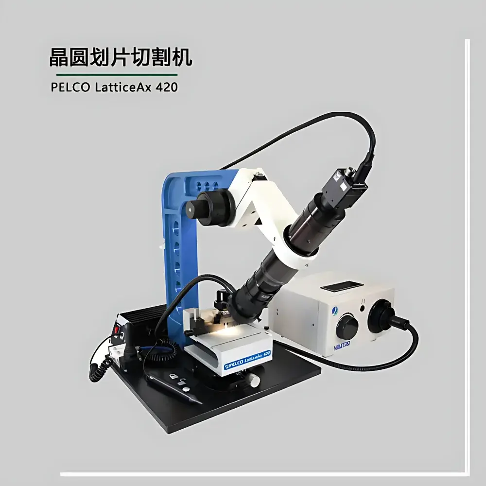
PELCO LatticeAx 420 Wafer Dicing Saw
| Origin | USA |
|---|---|
| Manufacturer Type | Distributor |
| Origin Category | Imported |
| Model | PELCO LatticeAx 420 |
| Price Range | USD 0–15,000 |
| Maximum Scribe Speed | 500–600 mm/min |
| Application Scope | Laboratory Use |
| Positioning Accuracy | ±10 µm |
| Indentation Step Resolution | 5 µm |
| Optical Magnification | 0.58–7× (zoom, parfocal, monocular) |
| Camera | Color CCD |
| Diamond Scribing Tip | Polished Single-Point Diamond |
| Focusing Mechanism | Coarse + Fine Focus Stage |
| Footprint | Compact Industrial Platform |
Overview
The PELCO® LatticeAx 420 Wafer Dicing Saw is a precision scribing instrument engineered for laboratory-scale semiconductor sample preparation. Unlike full-scale automated dicing saws that rely on rotating diamond blades and coolant systems, the LatticeAx 420 employs a controlled mechanical scribing principle—using a polished single-point diamond tip to create micro-scale linear indentations (scribe lines) on brittle substrates such as silicon, GaAs, SiC, quartz, glass, and ceramic wafers. This non-rotating, low-force indentation method eliminates kerf loss, thermal stress, chipping, and subsurface damage commonly associated with blade-based dicing. Designed for prototyping, failure analysis, device isolation, and small-batch R&D workflows, the system delivers repeatable, high-fidelity scribe lines without requiring cleanroom-grade infrastructure or extensive operator training.
Key Features
- High-precision scribe positioning with ±10 µm stage repeatability, enabled by a motorized XYZ translation stage integrated with calibrated micrometer controls.
- Step-controlled indentation depth adjustment in 5 µm increments, allowing precise control over crack initiation depth for optimized post-scribe break strength and edge quality.
- Parfocal zoom optical system (0.58–7× magnification) with integrated color CCD camera, enabling real-time visual alignment and documentation of scribe paths at multiple working distances.
- Ergonomic, compact industrial platform (LatticeGear-compatible footprint) designed for benchtop integration in shared lab environments—no external vibration isolation or dedicated power conditioning required.
- Tool-free sample mounting via vacuum chuck and adjustable mechanical clamps; accommodates wafer diameters from 50 mm to 200 mm and irregularly shaped substrates up to 100 × 100 mm.
- Full backward compatibility with LatticeAx 120 functional architecture—including firmware logic, calibration routines, and user interface conventions—ensuring seamless workflow migration and technician cross-training.
Sample Compatibility & Compliance
The LatticeAx 420 supports a broad range of rigid, brittle materials used in microelectronics, MEMS, photonics, and academic device research. Verified substrates include silicon (100), silicon-on-insulator (SOI), gallium arsenide (GaAs), silicon carbide (SiC), fused silica, borosilicate glass, alumina, and LTCC ceramics. All scribe parameters—including tip load, dwell time, and traverse speed—are fully configurable per material class to comply with ASTM F1530 (Standard Guide for Mechanical Scribing of Semiconductor Wafers) and JEDEC JESD22-A110 (Mechanical Shock). The system’s manual operation mode meets GLP documentation requirements when paired with external timestamped image capture and operator log entries. No internal software qualifies as “electronic record” under FDA 21 CFR Part 11; however, exported scribe coordinates and camera images are compatible with validated LIMS or ELN platforms.
Software & Data Management
The LatticeAx 420 operates via an embedded microcontroller-driven interface with tactile push-button navigation and OLED status display—eliminating reliance on PC-hosted software or proprietary drivers. All operational parameters (X/Y/Z coordinates, magnification level, scribe speed, dwell duration) are stored in non-volatile memory with timestamped session logs. Image capture from the integrated color CCD is routed directly to USB 2.0 output for transfer to external workstations. Raw coordinate data exports as CSV files for traceability, statistical process control (SPC), or integration into MATLAB/Python-based metrology pipelines. Optional LatticeGear Bridge software (sold separately) enables batch script generation, multi-site pattern replication, and overlay alignment against reference SEM or optical microscope images.
Applications
- Rapid prototyping of discrete devices from full wafers prior to tape-and-frame packaging.
- Controlled cleaving of photonic integrated circuits (PICs) and laser bars for facet characterization.
- Preparation of test dies for electrical probing, TEM lamella extraction, or cross-sectional SEM analysis.
- Low-volume production of sensor arrays where blade dicing would induce unacceptable microcracking.
- Teaching laboratories demonstrating fracture mechanics, brittle material processing, and semiconductor fabrication fundamentals.
- Failure analysis labs isolating defective die while preserving adjacent functional units for comparative testing.
FAQ
Is the LatticeAx 420 compliant with ISO 9001 or ISO/IEC 17025 laboratory accreditation requirements?
Yes—when operated within documented procedures and maintained per PELCO’s Calibration and Maintenance Manual (Rev. 4.2), the system supports traceable measurement uncertainty budgets for scribe line placement and depth. Internal calibration checks use NIST-traceable gauge blocks and certified step-height standards.
Can the diamond scribing tip be replaced in-house, and what is its typical service life?
Yes—the tip is field-replaceable using standard hex keys. Under normal lab usage (≤ 200 scribe lines/week on silicon), tip life exceeds 6 months. Tip wear is monitored visually via the zoom optics or quantitatively using profilometry on calibration scribe lines.
Does the system require compressed air, coolant, or special electrical grounding?
No—it operates on standard 100–240 VAC, 50/60 Hz input with internal EMI filtering. No auxiliary utilities are needed, making it suitable for temporary setups or mobile lab configurations.
What is the minimum feature size achievable with the LatticeAx 420?
The practical scribe line width is ~8–12 µm (dependent on substrate hardness and tip geometry), with inter-line spacing down to 25 µm achievable using fine-stage stepping and optical alignment. Sub-micron positioning resolution is not claimed—only ±10 µm stage repeatability per ISO 230-2.
Is remote operation or network connectivity supported?
Not natively. The unit lacks Ethernet, Wi-Fi, or RS-232 interfaces. However, third-party USB-to-Ethernet adapters may enable basic remote monitoring of the camera feed, though scribe execution remains local and manual.


