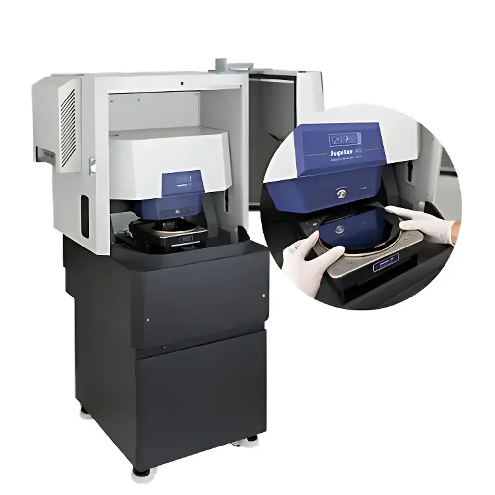
Oxford Instruments Asylum Research Jupiter XR Large-Sample Atomic Force Microscope
| Brand | Oxford Instruments |
|---|---|
| Origin | USA |
| Manufacturer Type | Authorized Distributor |
| Origin Category | Imported |
| Model | Jupiter XR |
| Price Range | USD 320,000 – 385,000 |
| Instrument Type | Atomic Force Microscope (AFM) |
| Application Class | Materials Science AFM |
| Position Detection Noise | 35 pm |
| Maximum Sample Diameter | 210 mm |
| XY Stage Travel Range | 200 mm × 200 mm |
| Scan Range | Up to 100 μm (full closed-loop) |
| Imaging Speed | 5–20× faster than conventional large-sample AFMs |
Overview
The Oxford Instruments Asylum Research Jupiter XR is a high-performance, large-sample atomic force microscope engineered for precision nanoscale characterization of industrially relevant specimens—particularly wafers, photomasks, semiconductor substrates, and advanced functional materials. Built upon Asylum Research’s proprietary Cypher platform architecture, the Jupiter XR implements a dual-stage scanning design: a high-speed, low-noise piezoelectric scanner (100 μm range, closed-loop feedback) mounted on a motorized 200 mm × 200 mm XY stage. This hybrid motion system enables seamless transition between macro-scale navigation and nanometer-resolution imaging without sample repositioning. Its position detection noise floor of 35 pm (RMS, in air) ensures exceptional sensitivity for quantitative topography, mechanical property mapping (e.g., modulus, adhesion), and electrical characterization (CAFM, KPFM, PFM). Designed for both academic laboratories and industrial R&D environments, the Jupiter XR complies with foundational metrology requirements for ISO/IEC 17025-compliant labs and supports traceable calibration protocols aligned with ASTM E2539 and ISO 25178-601.
Key Features
- Dual-stage scanning architecture: Combines a high-bandwidth 100 μm piezoscanner with a precision-motorized 200 mm XY stage for rapid macro-to-nano workflow integration.
- Sub-angstrom height resolution: Achieved via low-drift, low-noise optical beam deflection (OBD) detection and active environmental vibration isolation.
- Modular head design: Supports interchangeable probe holders, liquid cells, temperature-controlled stages (−30 °C to +250 °C), and integrated optical access for correlative microscopy.
- Automated tip approach and scan setup: Reduces operator dependency through AI-assisted parameter optimization and real-time feedback during coarse approach and engagement.
- Robust mechanical architecture: All-metal frame with granite base and passive damping minimizes thermal drift and acoustic coupling—critical for long-duration, multi-region measurements on 200 mm wafers.
Sample Compatibility & Compliance
The Jupiter XR accommodates samples up to 210 mm in diameter—including full 200 mm silicon wafers, glass substrates, flexible OLED panels, and composite laminates—without edge clipping or field-of-view limitation. Its open-stage geometry permits direct mounting of custom fixtures, electrochemical cells, or in situ stress-testing rigs. The system meets essential safety and electromagnetic compatibility standards per IEC 61000-6-3 and IEC 61000-6-4. For regulated environments, optional audit-trail logging, electronic signature support, and 21 CFR Part 11–compliant software modules are available to satisfy GLP/GMP documentation requirements in semiconductor process development and medical device material qualification.
Software & Data Management
Acquired and analyzed using Asylum Research’s Interactive Microscopy Platform (IMP) software, the Jupiter XR delivers intuitive, scriptable, and reproducible workflows. IMP features real-time data streaming, multi-channel synchronized acquisition (topography, phase, current, dissipation), and automated stitching of >100-tile mosaic maps across the full 200 mm stage. All raw data are stored in vendor-neutral HDF5 format with embedded metadata (scan parameters, calibration constants, timestamp, user ID). Batch processing pipelines support ISO 25178 surface texture analysis, grain boundary detection via machine learning segmentation, and export to third-party platforms including MATLAB, Python (via asylumpy), and Metrology Software Suite (MSS). Audit logs record every user action—including parameter changes, file exports, and report generation—for full traceability.
Applications
- Semiconductor metrology: Critical dimension (CD) uniformity, trench depth profiling, and post-CMP surface roughness assessment on 200 mm wafers.
- Advanced packaging: Interfacial delamination analysis in fan-out wafer-level packaging (FOWLP) and underfill void detection.
- Energy materials: Nanomechanical mapping of solid-electrolyte interphase (SEI) layers in battery electrodes and grain-resolved conductivity in perovskite solar cell absorbers.
- Biomedical polymers: Surface degradation kinetics of resorbable scaffolds under physiological immersion conditions.
- Hard-coating QC: Adhesion quantification via nano-scratch testing combined with in situ friction force imaging.
FAQ
What is the maximum sample thickness compatible with the Jupiter XR?
Standard configuration supports samples up to 50 mm thick; optional extended-Z kits increase this to 100 mm.
Does the Jupiter XR support vacuum or controlled-atmosphere operation?
Yes—optional environmental chambers enable operation under inert gas (N₂, Ar), low-humidity dry air (<5% RH), or moderate vacuum (10⁻² mbar).
Can the system perform automated defect review across a full 200 mm wafer?
Yes—integrated pattern recognition algorithms coupled with stage-level coordinate referencing enable repeatable site-specific imaging at predefined die locations.
Is third-party probe compatibility supported?
The Jupiter XR accepts standard cantilevers with 125 µm × 125 µm × 5 µm chip dimensions and nominal spring constants from 0.01 N/m to 100 N/m; OEM probes are recommended for calibrated quantitative modes.
How is calibration traceability maintained for regulatory submissions?
NIST-traceable step-height standards (e.g., VLSI Standards S100 series) and certified roughness artifacts (ISO 25178-71) are supported; calibration certificates and uncertainty budgets are auto-generated within IMP.


