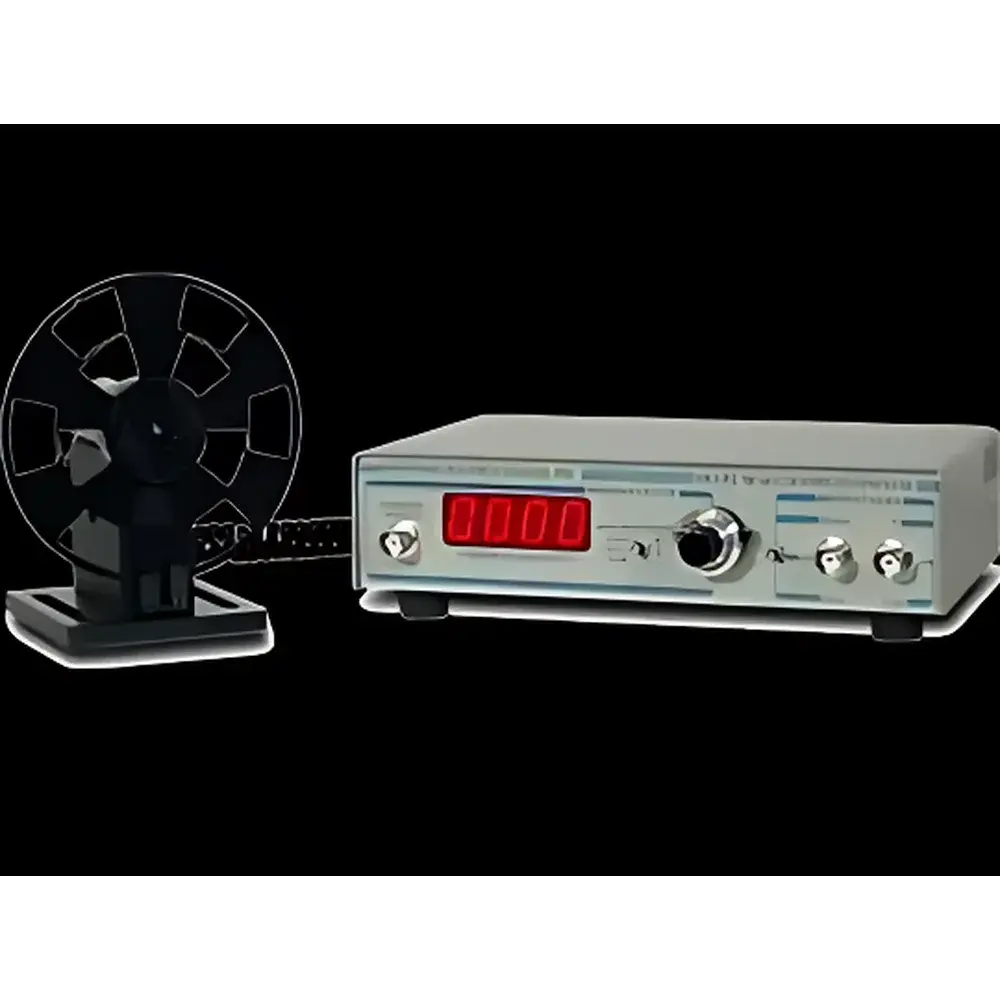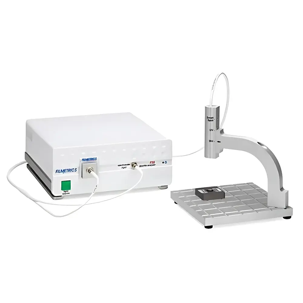
Filmetrics F20 Advanced Thin-Film Thickness Metrology System
| Brand | Filmetrics |
|---|---|
| Model | F20 |
| Measurement Range | 1 nm – 10 mm |
| Principle | Broadband Interferometric Reflectometry |
| Wavelength Range | Standard (UV-VIS-NIR, e.g., 190–1700 nm) |
| Measurement Speed | < 1 s per point |
| Output Parameters | Thickness, Refractive Index (n), Extinction Coefficient (k), Surface Roughness (qualitative) |
| Interface | USB 2.0 to Windows™ PC |
| Software | FILMeasure 5.0 (with GLP-compliant audit trail, calibration logging, and multi-layer fitting) |
| Compliance | Supports ASTM E1938-22, ISO 15630-3, and FDA 21 CFR Part 11–ready configuration (optional electronic signatures & user access control) |
Overview
The Filmetrics F20 Advanced Thin-Film Thickness Metrology System is a benchtop, non-contact optical metrology instrument engineered for rapid, high-reproducibility measurement of thin-film thickness and optical constants across an exceptionally wide dynamic range—from atomic-scale monolayers (1 nm) up to optically thick coatings (10 mm). It operates on the principle of broadband interferometric reflectometry: a collimated beam of polychromatic light (typically spanning 190–1700 nm) is directed normal to the sample surface; interference patterns arising from reflections at multiple interfaces (e.g., air/film, film/substrate) are captured by an integrated high-resolution spectrometer. The resulting spectral reflectance curve contains oscillatory features whose periodicity, amplitude, and phase encode film thickness, complex refractive index (n + ik), and interfacial roughness. A physics-based least-squares fitting algorithm—grounded in the Fresnel equations and recursive transfer-matrix modeling—extracts these parameters with sub-nanometer resolution for ultrathin films and ±0.1% repeatability for thicker layers. Unlike mechanical or eddy-current methods, the F20 imposes no physical contact, requires no vacuum, and introduces no sample damage—making it ideal for inline QC, R&D prototyping, and failure analysis in high-value manufacturing environments.
Key Features
- Single-shot, non-destructive measurement of thickness (1 nm – 10 mm), n/k dispersion, and qualitative roughness in under one second
- Modular wavelength configurations: F20-UV (190–1100 nm) for sub-5 nm dielectrics; F20-NIR (400–1700 nm) for polymer stacks, photoresists, and opaque multilayers
- Integrated spectrometer and stabilized tungsten-halogen + deuterium light source with thermal management for drift-free operation over 8+ hour sessions
- Motorized, multi-position SS-3 sample stage with manual Z-focus and optional auto-focus (±1 µm repeatability)
- FILMeasure 5.0 software featuring real-time curve fitting, multi-layer stack modeling (up to 10 layers), dispersion library (Cauchy, Sellmeier, Tauc), and batch processing for wafer-level data
- Fully compliant USB 2.0 interface; no external power supply or PCIe card required—operates directly from Windows 10/11 host
Sample Compatibility & Compliance
The F20 measures virtually all non-metallic and semi-transparent materials—including silicon dioxide, silicon nitride, ITO, Al₂O₃, SiC, DLC, PMMA, parylene-C, SU-8, CIGS, perovskites, and biological polymer films—on rigid or flexible substrates (Si, glass, quartz, sapphire, PET, PI). Metallic films (e.g., Au, Al) are measurable only when capped or embedded within dielectric stacks. The system supports ASTM E1938-22 (Standard Test Method for Measuring Thickness of Transparent Films Using Spectroscopic Reflectometry) and aligns with ISO 15630-3 for optical characterization of coated substrates. For regulated environments, FILMeasure 5.0 offers optional 21 CFR Part 11 compliance packages—including role-based user authentication, electronic signatures, immutable audit trails, and calibration certificate generation—enabling deployment in GMP/GLP laboratories and medical device manufacturing facilities.
Software & Data Management
FILMeasure 5.0 is a native 64-bit Windows application built on a modular architecture that separates acquisition, modeling, and reporting engines. It includes a fully scriptable API (Python, MATLAB, LabVIEW), enabling integration into automated test sequences and MES/SCADA systems. All raw spectra, fit residuals, parameter covariance matrices, and instrument metadata are stored in HDF5 format—ensuring long-term readability and FAIR data principles adherence. Batch analysis tools support wafer maps (CSV/XLSX export), statistical process control (SPC) charting (X-bar/R, Cpk), and pass/fail thresholding against design specifications. Optional FILMeasure Standalone permits offline analysis of field-collected datasets without requiring instrument connection—critical for remote troubleshooting and cross-site collaboration.
Applications
- Semiconductor fabrication: gate oxide, hard mask, and ARC layer verification on 200 mm/300 mm wafers
- Display manufacturing: RGB pixel bank, TFT passivation, and touch sensor ITO thickness uniformity mapping
- Optical coating QC: anti-reflective, beam-splitter, and filter stack composition validation
- MEMS/NEMS development: structural layer thickness and stress-induced curvature correlation
- Photovoltaics: CIGS absorber, CdS buffer, and encapsulation layer thickness optimization
- Biomedical device R&D: hydrogel swelling kinetics, drug-eluting polymer coating release profiling, and biosensor functionalization monitoring
FAQ
What minimum film thickness can the F20 resolve?
The F20 achieves reliable thickness quantification down to 1 nm for high-contrast dielectrics (e.g., SiO₂ on Si) using UV-enhanced optics and advanced noise suppression algorithms.
Can the F20 measure multilayer stacks?
Yes—FILMeasure 5.0 supports full forward-modeling of up to 10-layer stacks with independent thickness, n/k, and roughness parameters per layer.
Is vacuum or nitrogen purge required?
No—ambient air operation is standard; optional purge ports are available for moisture-sensitive measurements (e.g., hygroscopic polymers).
How is calibration performed and maintained?
Factory calibration uses NIST-traceable thickness standards; users perform routine verification with supplied SiO₂-on-Si reference wafers and generate calibration reports compliant with ISO/IEC 17025 requirements.
Does the system support automated stage integration?
Yes—the F20 communicates via ASCII over USB and supports third-party XY stages through TTL-triggered acquisition and coordinate mapping in FILMeasure.