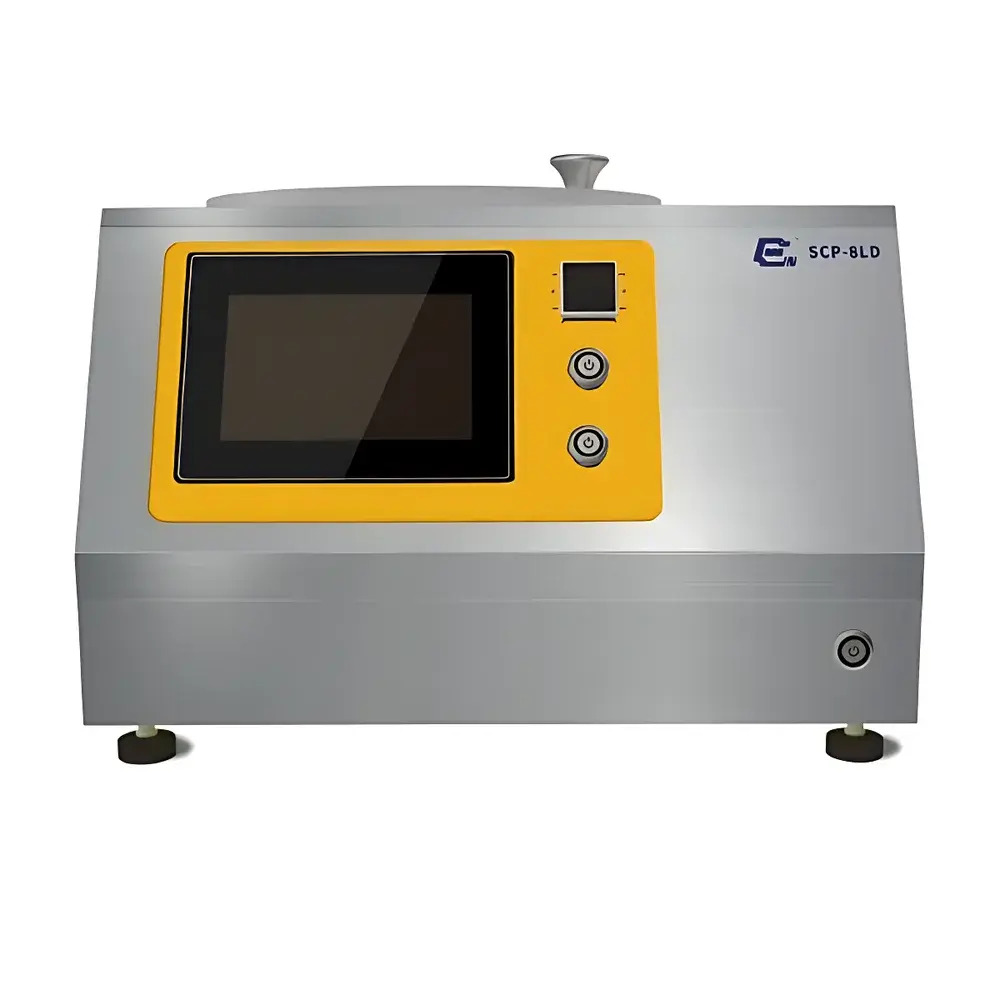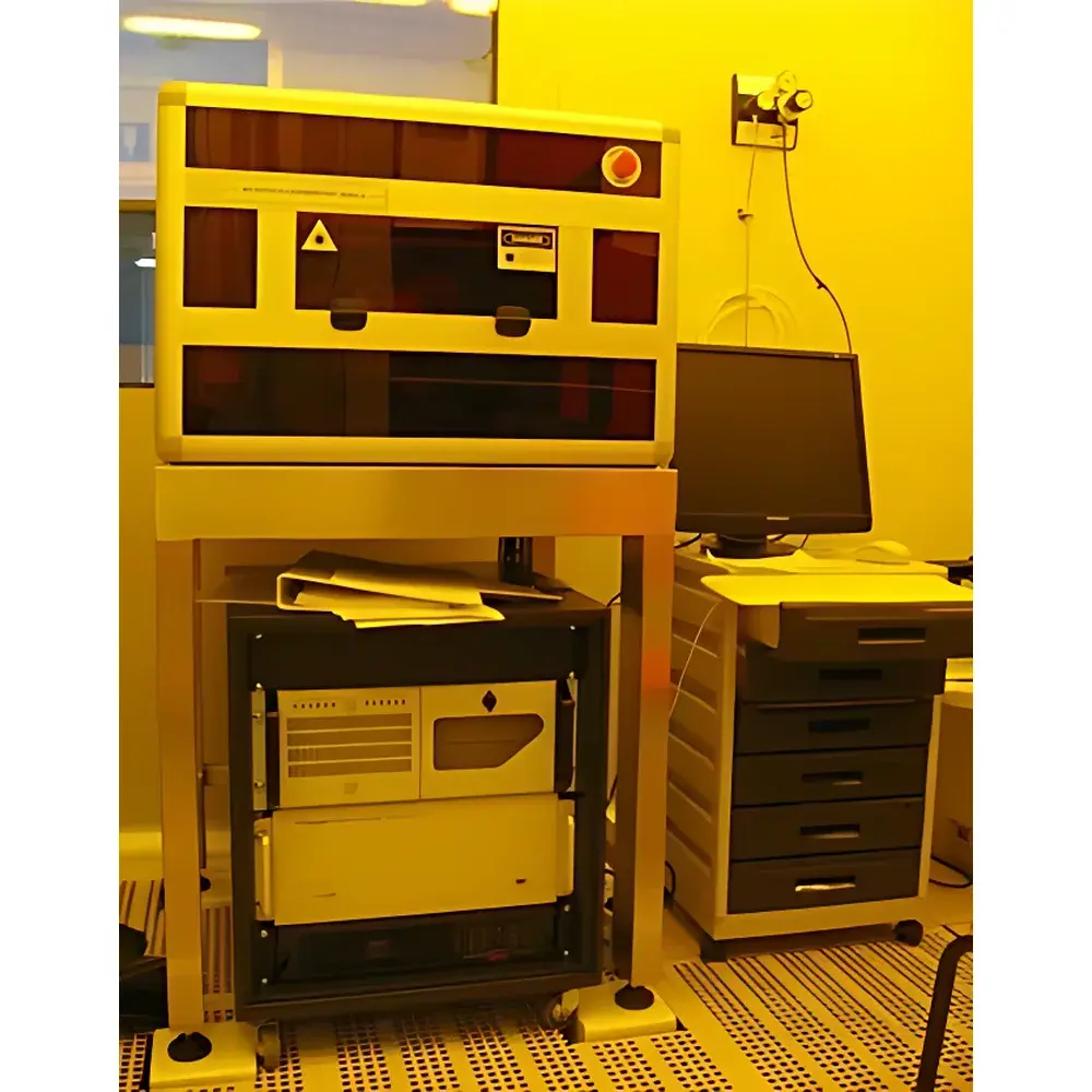
Microtech LW405D/LW405E Ultra-High-Resolution Maskless Direct-Write Lithography System
| Brand | MICROTECH |
|---|---|
| Origin | Italy |
| Model | LW405D / LW405E |
| Minimum Feature Size | 0.3–0.5 µm (material- and environment-dependent) |
| Beam Acceleration Voltage | 30 kV |
| Wavelength Options | 405 nm, 375 nm, 365 nm, and optional 213 nm DUV source |
Overview
The Microtech LW405D and LW405E are ultra-high-resolution maskless direct-write lithography systems engineered for precision nanofabrication in academic research, pilot-line development, and low-to-medium volume semiconductor manufacturing. Unlike conventional photolithography tools that rely on physical masks, these systems employ a digitally controlled laser scanning architecture—based on galvanometric mirror positioning and high-stability optical path design—to project patterned exposure directly onto photoresist-coated substrates. The core exposure mechanism utilizes focused UV laser beams (standard 405 nm, with optional 375 nm, 365 nm, and 213 nm deep-UV sources), enabling sub-500 nm feature resolution under optimized resist and environmental conditions. The 30 kV beam acceleration voltage specification listed refers to the electron-optical subsystem in hybrid configurations; however, the LW405 series is fundamentally a *laser-based* platform—not an electron-beam system—despite its classification under “Electron Beam Lithography System” in certain regional catalogs (a legacy categorization reflecting early Microtech’s dual-technology heritage). This distinction is critical for users evaluating vacuum requirements, throughput, and resist compatibility.
Key Features
- Multi-wavelength exposure capability: Standard 405 nm diode laser, upgradable to 375 nm and 365 nm UV sources, plus optional 213 nm DUV module—unique in the maskless lithography market—enabling high-resolution direct patterning of PMMA and other DUV-sensitive resists without e-beam infrastructure.
- Digital pattern generation with real-time correction: Vector-based writing engine supports sub-pixel alignment accuracy, dynamic focus compensation, and stage-synchronized exposure timing for consistent dose delivery across large fields.
- Modular platform architecture: Configurable for R&D (LW405D), production-integrated (LW405E), or multi-beam parallel processing (custom up to 8-head array), supporting wafer sizes up to 800 mm × 800 mm with thermal and mechanical stability compliant with ISO 14644-1 Class 5 cleanroom integration.
- High positional reproducibility: Closed-loop air-bearing XY stage with interferometric feedback ensures ≤ ±25 nm overlay accuracy over 100 mm × 100 mm fields—validated per ISO 9283 and ASTM E2482 standards.
- Environmental adaptability: Active vibration isolation and temperature-controlled optical bench enable stable operation in non-dedicated lab environments, reducing dependency on Class 10 or better cleanrooms for sub-micron work.
Sample Compatibility & Compliance
The LW405 series accommodates rigid and semi-flexible substrates including silicon wafers (up to 200 mm), fused silica, sapphire, glass, ITO-coated PET, and polymer foils. Resist compatibility spans standard g/i-line resists (e.g., S1805, AZ4620), chemically amplified resists (CARs), and high-resolution negative-tone resists (e.g., HSQ, ZEP520A) as well as DUV-optimized polymers (e.g., PMMA, CALIX). System software includes pre-validated process recipes aligned with SEMI E10, ISO/IEC 17025 calibration traceability, and GLP-compliant audit trails. Optional FDA 21 CFR Part 11 modules support electronic signatures and secure data archiving for regulated environments.
Software & Data Management
Control is executed via Microtech’s proprietary LithoSuite™ v5.x software, a Windows-based application featuring CAD import (GDSII, OASIS, DXF), hierarchical pattern tiling, proximity effect correction (PEC), and dose modulation algorithms. All exposure logs—including stage position, laser power, ambient temperature/humidity, and shutter timing—are timestamped and stored in SQLite databases with SHA-256 hashing for integrity verification. Export formats include TIFF, SVG, and metrology-ready CSV files compatible with industry-standard inspection tools (e.g., KLA-CMS, Hitachi CG630). Remote monitoring and diagnostics are supported via TLS-encrypted HTTP API, enabling integration into factory MES platforms.
Applications
- Maskless fabrication of photomasks and reticles for prototyping and small-batch optical lithography
- Direct-write fabrication of diffractive optical elements (DOEs), metasurfaces, and plasmonic nanostructures
- Multi-layer alignment and overlay lithography for MEMS/NEMS, RF-MEMS switches, and inertial sensors
- Microfluidic channel patterning in PDMS, COC, and cyclic olefin polymer (COP) substrates
- Grayscale lithography for 3D micro-optics and microlens arrays using tone mapping and variable dose control
- Surface photochemistry patterning for biosensor functionalization and guided cell adhesion studies
- Graphene device fabrication—including Hall bar structures, Josephson junctions, and quantum dot arrays—on Si/SiO₂ and hBN substrates
FAQ
Is the LW405 an electron-beam or laser-based system?
The LW405 series is fundamentally a laser direct-write platform. While Microtech historically developed both e-beam and laser technologies, the LW405 uses solid-state UV lasers—not electron optics—and requires no vacuum chamber.
What determines the minimum achievable linewidth?
Resolution depends on laser wavelength, numerical aperture of the projection lens, photoresist contrast, development uniformity, and environmental stability. Typical best-case resolution is 0.3 µm in PMMA with 213 nm DUV; 0.5 µm is routinely achieved with 405 nm in standard positive resists.
Can the system be integrated into an existing cleanroom automation line?
Yes. LW405E models support SECS/GEM communication protocols, SMIF interface options, and robotic wafer handling integration per SEMI E47.1 specifications.
Does the 213 nm DUV option require special safety infrastructure?
Yes. DUV operation mandates Class 3B laser safety interlocks, UV-absorbing enclosures, and operator training per IEC 60825-1. Microtech provides full compliance documentation and installation validation support.
Is overlay metrology supported natively?
Overlay accuracy is verified using built-in fiducial recognition and cross-correlation algorithms. For traceable metrology, optional integration with external CD-SEM or optical overlay tools (e.g., Nanometrics Atlas) is available via standardized data exchange APIs.