EULITHA AG Nanoimprint Master Template
| Brand | EULITHA AG |
|---|---|
| Origin | Germany |
| Manufacturer Type | Authorized Distributor |
| Origin Category | Imported |
| Model | Template |
| Pricing | Upon Request |
Overview
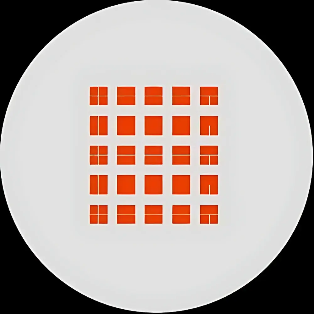
EULITHA AG Nanoimprint Master Templates are high-precision, silicon-based nanoscale pattern masters engineered for rapid prototyping, metrology reference, optical testing, and nanostructure replication via thermal or UV nanoimprint lithography (NIL). Fabricated using high-resolution electron-beam lithography (EBL) and reactive ion etching (RIE), these templates deliver deterministic sub-100 nm feature fidelity on single-crystal silicon substrates. Unlike process-intensive in-house patterning, EULITHA’s standardized master templates eliminate the need for beam-time allocation, mask alignment, and etch optimization—enabling researchers and process engineers to bypass months of process development and proceed directly to imprint validation, optical characterization, or plasmonic device evaluation. Each template is designed with strict dimensional control over period, line/space ratio (duty cycle), pillar/hole diameter, depth, and lattice symmetry (square, rectangular, hexagonal, or rhombic), ensuring traceable performance across academic labs, semiconductor R&D centers, and photonics foundries.
Key Features
- Single-crystal silicon substrate (standard thickness: 0.675 ± 0.050 mm; optional 0.5 mm or 1.0 mm variants available)
- High-fidelity nanofabrication: EBL-written patterns followed by anisotropic RIE etching for vertical sidewalls and uniform depth profiles
- Precision metrology-grade tolerances: period accuracy better than ±0.5%, critical dimension (CD) variation ≤ ±10% for diameters/line widths, depth variation ≤ ±15%
- Low-defect surface: <1% defective area per active region; scratch/dig specifications compliant with MIL-PRF-13830B Class 60–40 for optical-grade variants
- Scalable form factors: standard chips (8 × 8.3 mm, 12.5 × 12.5 mm, 20 × 9 mm, up to 25 × 25 mm), 2×2 cm² master stamps, 4-inch (100 mm) and 6-inch (150 mm) wafers
- Multi-lattice support: linear gratings, square/rectangular lattices, hexagonal lattices, rhombic lattices, and multi-period composite patterns
- Material compatibility: optimized for Si, fused silica (quartz), and low-Tg polymer resists (e.g., mr-NIL210, Optool UV-NIL)
Sample Compatibility & Compliance
EULITHA master templates are compatible with industry-standard nanoimprint platforms including EVG®620, Canon NI-100, and Obducat Nanoimprinter systems. All silicon templates meet ISO 10110-7 surface quality requirements for optical substrates and conform to SEMI Standard F42 for semiconductor wafer flatness and edge exclusion. For regulated environments, templates support GLP/GMP-aligned documentation packages—including certificate of conformance, metrology reports (traceable to PTB or NIST standards), and batch-specific SEM cross-section verification. While not classified as medical devices, templates used in FDA-regulated photonic biosensor development comply with relevant portions of 21 CFR Part 11 when paired with validated data acquisition software.
Software & Data Management
No proprietary software is required to utilize EULITHA templates. However, full metrological traceability is supported through standardized reporting formats: GDSII layout files (for CAD verification), calibrated SEM image stacks (with scale bars), and Excel-based dimensional summary sheets (including mean ± 3σ for period, CD, and depth across ≥5 field positions). Customers may integrate templates into automated inspection workflows using common machine vision tools (e.g., KLA eDR72xx, Bruker Dektak XTL) or open-source analysis pipelines (Python-based PyImageJ + NanoMorph). Batch-level documentation is archived for ≥10 years and available upon request for audit readiness.
Applications
- Optical Metrology: Calibration standards for scatterometry (RCWA), ellipsometry, and broadband reflectance spectroscopy
- Nanophotonics Research: Plasmonic arrays, metasurface unit cells, photonic crystal slabs, and guided-mode resonance filters
- Semiconductor Process Development: NIL process window studies, defect density benchmarking, and stamp lifetime evaluation
- Academic Teaching & Training: Hands-on NIL lab modules, diffraction physics demonstrations, and AFM/SEM imaging practice substrates
- Biosensing Platform Fabrication: Surface-enhanced Raman scattering (SERS) substrates, nanopore sensor arrays, and microfluidic-nanostructured hybrid devices
- Advanced Packaging: Alignment marks, fiducial patterns, and hierarchical structures for heterogeneous integration
FAQ
Are these templates suitable for high-volume production imprinting?
Yes—EULITHA templates are fabricated on prime-grade Czochralski silicon wafers with controlled resistivity and surface roughness (1,000 imprint cycles under optimized release conditions. For production use, we recommend quartz variants for UV-NIL durability.
Can I request custom dimensions or non-standard periods?
Custom designs are supported under NRE agreements. Minimum order quantities apply for non-standard geometries; typical lead time is 6–8 weeks from layout approval.
What is the maximum aspect ratio achievable on silicon templates?
Aspect ratios up to 10:1 are routinely achieved (e.g., 1000 nm depth / 100 nm linewidth); higher ratios require quartz substrates or specialized etch chemistries and are evaluated case-by-case.
Do you provide cross-sectional SEM images or AFM topography data?
Yes—each shipment includes a metrology report with representative cross-sectional SEMs and height-profile AFM scans for the specified pattern type and depth.
How are templates cleaned and packaged?
Templates undergo rigorous RCA-1/RCA-2 cleaning, nitrogen-dry purge, and vacuum-sealed packaging in Class 100 cleanroom environments. Each unit is shipped with a certified particulate count report (<10 particles ≥0.5 µm per cm²).


