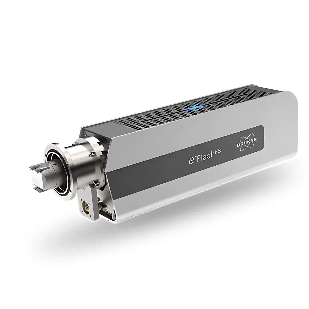
Bruker QUANTAX EBSD System
| Brand | Bruker |
|---|---|
| Origin | Germany |
| Manufacturer Type | Authorized Distributor |
| Origin Category | Imported |
| Model | QUANTAX EBSD |
| Pricing | Upon Request |
| CCD Camera Resolution | 640 × 480 pixels |
| Maximum Stage Speed | 10 mm/s |
| Spatial Resolution | 1.5 nm |
| Angular Resolution | 0.1° |
Overview
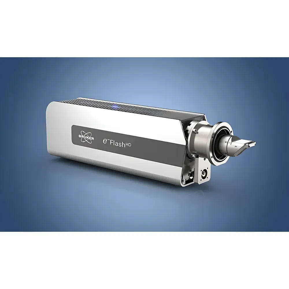
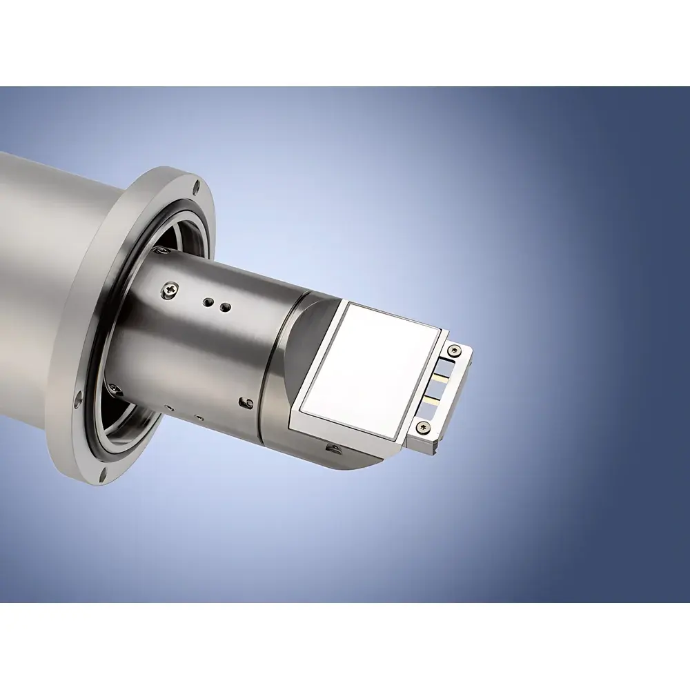
The Bruker QUANTAX EBSD System is a high-performance electron backscatter diffraction (EBSD) solution engineered for crystallographic characterization in scanning electron microscopes (SEM). Operating on the fundamental principle of elastic backscattering of high-energy electrons from crystalline lattice planes, the system captures Kikuchi diffraction patterns to determine grain orientation, phase identification, misorientation distribution, and local strain at sub-micron to nanoscale spatial resolution. Integrated with Bruker’s OPTIMUS TKD (Transmission Kikuchi Diffraction) detector, the QUANTAX platform extends analytical capability to ultra-thin and beam-sensitive specimens—enabling robust crystallographic mapping under low-dose conditions (e.g., ≤1 nA probe current) without compromising pattern quality or acquisition speed. Its compatibility with immersion lens SEM configurations ensures optimal signal collection efficiency even at accelerating voltages as low as 5 kV, making it particularly suited for advanced materials research including nanocrystalline alloys, 2D materials, and cross-sectional TEM lamellae prepared via FIB-SEM.
Key Features
- Sub-nanometer spatial resolution (1.5 nm) achieved through optimized phosphor screen design, high-sensitivity CCD detection, and real-time pattern center calibration.
- High angular resolution (0.1°) enabling precise misorientation analysis, subgrain boundary detection, and reliable identification of deformation twins and stacking faults.
- Seamless integration with Bruker’s OPTIMUS TKD detector—the only commercially available TKD solution fully compatible with high-resolution immersion-mode SEMs.
- ARGUS™ integrated camera system provides automatic pattern quality assessment, live indexing feedback, and real-time drift correction during long-duration mapping sessions.
- Motorized stage with 10 mm/s maximum translation speed supports rapid area navigation and large-area mosaic mapping while maintaining positional repeatability within ±0.5 µm.
- Low-current operation capability (down to 0.5–1 nA) minimizes beam damage on sensitive nanostructures and insulating samples, preserving structural integrity during extended acquisitions.
Sample Compatibility & Compliance
The QUANTAX EBSD system accommodates a broad range of conductive and non-conductive solid-state specimens—including metals, ceramics, semiconductors, geological minerals, and thin-film heterostructures—provided appropriate surface preparation (e.g., ion milling or electropolishing) is performed to achieve atomically flat, strain-free surfaces. For insulating samples, carbon or chromium coating (≤5 nm thickness) is recommended to prevent charging artifacts without significantly degrading pattern contrast. The system complies with international standards relevant to microstructural analysis, including ASTM E112 (grain size measurement), ISO 13077 (EBSD terminology and methodology), and ASTM E3097 (crystallographic orientation mapping). Data acquisition and processing workflows support GLP/GMP-aligned documentation requirements, including full audit trails, user authentication, and metadata embedding compliant with FDA 21 CFR Part 11 when deployed in regulated environments.
Software & Data Management
Acquisition and post-processing are managed through Bruker’s ESPRIT software suite, which delivers intuitive workflow automation, batch indexing, phase library management (with built-in ICDD PDF-4+ database integration), and customizable scripting via Python API. All raw pattern files (.h5 or .bmp), indexed maps (.ctf/.ang), and metadata (beam energy, working distance, tilt angle, detector geometry) are stored in standardized formats supporting third-party interoperability (e.g., MTEX, Dream.3D, OIM Analysis). Data security features include role-based access control, encrypted project archives, and optional networked license management for multi-user laboratory deployments. Export options include publication-ready vector graphics (SVG/EPS), quantitative statistical reports (CSV/Excel), and 3D reconstruction-ready datasets for correlative FIB-SEM tomography.
Applications
- Quantitative texture analysis in rolled aluminum alloys and Ni-based superalloys for aerospace component qualification.
- Nanoscale grain boundary engineering studies in oxide dispersion strengthened (ODS) steels under irradiation conditions.
- Phase transformation kinetics mapping in lithium-ion battery cathode materials (e.g., NMC, LFP) during in situ electrochemical cycling.
- Crystallographic defect characterization in GaN-on-Si epitaxial layers for power electronics reliability assessment.
- Strain mapping across semiconductor heterojunctions using high-resolution EBSD-based lattice parameter deviation analysis.
- Automated mineral phase identification and provenance analysis in geological thin sections for resource exploration.
FAQ
What SEM models are compatible with the QUANTAX EBSD system?
The system is validated for integration with major SEM platforms from Thermo Fisher Scientific (Verios, Apreo), Zeiss (Sigma, GeminiSEM), JEOL (JSM-7900F, JSM-IT800), and Hitachi (SU-series), provided standard EBSD port geometry and vacuum interlock protocols are supported.
Can the QUANTAX EBSD system perform dynamic in situ experiments?
Yes—when coupled with compatible heating, cooling, or mechanical testing stages, the system supports time-resolved EBSD mapping with frame rates up to 100 Hz (depending on pattern resolution and binning), enabling real-time observation of recrystallization, martensitic transformation, or creep deformation.
Is TKD mode compatible with standard EBSD sample preparation methods?
No—TKD requires electron-transparent specimens (typically <100 nm thick), prepared via FIB lift-out or precision ion polishing. Standard bulk EBSD samples (polished to ~0.02 µm finish) are unsuitable for TKD but remain fully compatible with conventional EBSD mode.
How does ARGUS imaging enhance data reliability?
ARGUS continuously monitors pattern sharpness, background noise, and beam drift during acquisition, automatically adjusting exposure time and triggering re-acquisition if quality thresholds fall below user-defined criteria—reducing manual intervention and improving dataset consistency across multi-day campaigns.


