HCP PPLN Waveguide Chips
| Brand | HCP (Longcai Technology) |
|---|---|
| Origin | Taiwan |
| Manufacturer Type | Authorized Distributor |
| Product Category | Domestic (China-sourced) |
| Model | PPLN Waveguide Chips |
| Pricing | Upon Request |
Overview
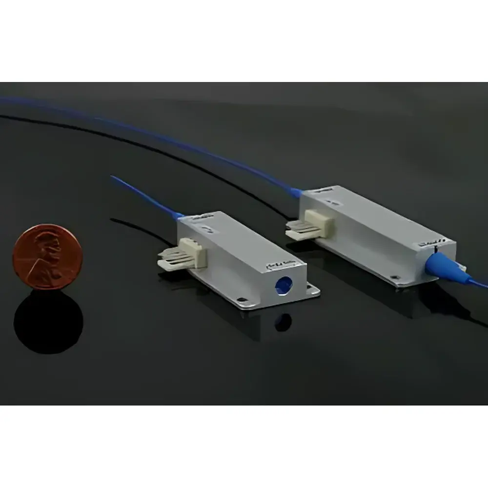
HCP PPLN Waveguide Chips are monolithic, periodically poled lithium niobate (PPLN) devices engineered for high-efficiency nonlinear optical frequency conversion via quasi-phase-matching (QPM). Unlike bulk PPLN crystals—optimized for high-power continuous-wave or pulsed applications—these integrated waveguide chips confine light in a sub-micron transverse mode, enabling enhanced optical intensity and extended interaction lengths within compact footprints. The waveguides support both uniform and chirped QPM grating designs, allowing precise tailoring of phase-matching bandwidth, group-velocity dispersion, and spectral acceptance for advanced parametric processes including second-harmonic generation (SHG), sum-frequency generation (SFG), difference-frequency generation (DFG), optical parametric amplification (OPA), optical parametric generation (OPG), and optical parametric oscillation (OPO). Operating across a broad spectral range—from visible (450 nm) to mid-infrared (11 µm) and extendable into THz upon custom design—the chips serve as core components in quantum photonics, spectroscopic sensing, ultrafast laser systems, and telecom-band wavelength conversion.
Key Features
- Two waveguide fabrication platforms: proton-exchange (PE) and ridge-type structures—both fabricated on congruent or stoichiometric PPLN substrates
- Ridge waveguides offer superior optical damage threshold (>1 GW/cm² for ns pulses), broader operational wavelength tolerance, and reduced propagation loss compared to conventional ion- or proton-diffused waveguides
- Engineered modal confinement with mode field diameters (MFD) ranging from 4.9 × 4.1 µm² to 5.65 × 4.35 µm², supporting single-mode operation at target wavelengths
- Controlled numerical aperture (NA) profiles: 0.13–0.30 (depending on waveguide type and wavelength band), optimized for low-loss coupling with standard SMF-28 or polarization-maintaining fibers
- Propagation losses as low as 0.7 dB/cm (typical) across visible-to-near-IR bands; higher values (up to 1.1 dB/cm) observed in mid-IR configurations due to phonon absorption
- Normalized conversion efficiency up to 250 %/W/cm² (at 532 nm → 1064 nm SHG), scalable with pump intensity and interaction length
- Thermal tuning coefficients ranging from ~2.5 °C/nm (mid-IR) to ~13 °C/nm (blue-green), enabling precise temperature-stabilized phase matching
Sample Compatibility & Compliance
All HCP PPLN waveguide chips comply with standard cleanroom handling protocols (Class 1000 or better) and are packaged in nitrogen-purged, static-dissipative containers. Devices are compatible with commercial fiber-coupled modules, free-space optical benches, and OEM integration into laser systems requiring RoHS-compliant components. While not certified to ISO 9001 or IEC 61215 by default, full traceability of substrate origin (Taiwan-sourced LN wafers), poling uniformity data (±0.5% domain period variation), and post-fabrication characterization reports (including near-field MFD scans and spectral response curves) are available upon request. Custom devices may be qualified per customer-specific requirements aligned with GLP documentation practices for academic or industrial R&D use.
Software & Data Management
HCP provides comprehensive technical datasheets and application notes—not proprietary software—for all standard and custom waveguide products. Each chip is supplied with a unique serial identifier linked to its measured performance parameters (MFD, propagation loss, normalized efficiency, thermal tuning slope). For system-level integration, users are supported with MATLAB- and Python-compatible lookup tables mapping pump/output wavelength pairs to optimal temperature setpoints and poling period values. No embedded firmware or driver software is included, as these are passive dielectric components requiring external laser sources, temperature controllers (e.g., Thorlabs TED200C or Wavelength Electronics LDTC series), and alignment stages.
Applications
- Compact visible-light generation (e.g., 532 nm, 488 nm) via SHG of diode-pumped solid-state lasers
- Mid-IR spectroscopy sources (3–5 µm) using DFG between telecom-band pumps (1550 nm + 1650 nm)
- Entanglement photon-pair generation in spontaneous parametric down-conversion (SPDC) for quantum optics experiments
- Frequency comb extension and calibration through cascaded SFG/DFG in multi-stage waveguide arrays
- OEM integration into portable gas analyzers leveraging OPO-based broadband mid-IR output
- Ultrafast pulse shaping and compression using chirped-QPM waveguides with engineered group-delay dispersion
FAQ
What is the typical lead time for custom PPLN waveguide orders?
Standard catalog items ship within 2–3 weeks after order confirmation. Custom designs—including nonstandard poling periods, ridge geometries, or AR-coating specifications—require 8–12 weeks for fabrication, poling verification, and optical characterization.
Do you provide fiber-pigtailed versions?
Yes—HCP offers optional single-mode or polarization-maintaining fiber pigtailing with FC/APC or FC/PC connectors. Alignment tolerances are ±0.5 µm lateral and ±1° angular; coupling efficiencies exceed 70% (typical) for matched MFD configurations.
Can these waveguides operate under vacuum or cryogenic conditions?
Ridge waveguides demonstrate mechanical stability down to 77 K and are routinely used in cryo-cooled quantum optics setups. Thermal expansion mismatch between LN and silica fiber remains the primary constraint below 100 K; custom mounting solutions are available upon consultation.
Is there a minimum order quantity (MOQ) for standard products?
No MOQ applies to standard catalog items; single-unit orders are accepted. Volume pricing begins at quantities ≥5 units per serial number.
How is poling uniformity verified before shipment?
Each wafer undergoes nondestructive second-harmonic microscopy (SHM) mapping across the full grating region. Final chips are selected only if domain inversion uniformity meets ±0.5% period deviation over the active length, with full SHM image archives provided upon request.


