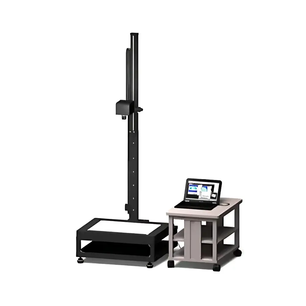
Photonic Lattice PA-300-XL Wafer Birefringence and Stress Mapping System
| Brand | Photonic Lattice |
|---|---|
| Origin | Japan |
| Model | PA-300-XL |
| Measurement Wavelength | 520 nm |
| Birefringence Range | 0–130 nm |
| Minimum Resolution | 0.001 nm |
| Repeatability | <0.1 nm |
| Field of View (Standard) | 40×48 mm to 240×320 mm |
| Polarization Camera | 2056×2464 pixels |
| Output Parameters | Retardance [nm], Fast-Axis Orientation [°], Stress-Converted Value [MPa] (optional) |
| Optional Modules | Real-time Analysis Software, Lens Aberration Analysis Software, External Control Interface, Interchangeable Lens Kits |
Overview
The Photonic Lattice PA-300-XL is a high-resolution, full-field birefringence mapping system engineered for non-contact, quantitative stress and optical anisotropy characterization of semiconductor wafers and optoelectronic substrates. It operates on the principle of polarization-resolved imaging interferometry, utilizing a fixed-polarization optical architecture with no moving filter wheels—ensuring mechanical stability, long-term calibration integrity, and immunity to vibration-induced artifacts. At its core, the system employs a monochromatic 520 nm LED illumination source coupled with a high-fidelity 2056×2464-pixel polarization camera to capture spatially resolved retardance (phase difference) and fast-axis orientation across the entire field of view in a single acquisition. This enables direct, pixel-level quantification of photoelastic response in crystalline materials such as silicon carbide (SiC), sapphire, and laser-grade Nd:YAG or Yb:YAG crystals—critical for identifying process-induced stress gradients, crystallographic defects, and wafer bow-related birefringence anomalies.
Key Features
- Single-shot full-field measurement: Captures complete birefringence maps within ≤3 seconds—eliminating scanning artifacts and enabling high-throughput inline or offline metrology.
- Fixed-optics design: No rotating waveplates or motorized polarizers—reducing maintenance requirements, eliminating alignment drift, and supporting stable operation under cleanroom environmental conditions.
- High spatial resolution: Standard FOV configurable from 40×48 mm up to 240×320 mm; optional lens kits extend flexibility for macro-scale wafer inspection or micro-scale localized defect analysis.
- Sub-picometer sensitivity: Achieves 0.001 nm minimum resolvable retardance with repeatability better than ±0.1 nm—enabling detection of sub-surface dislocation clusters and epitaxial strain fields.
- Direct stress conversion: Optional calibration module supports quantitative transformation of measured retardance into residual stress values (MPa) using material-specific photoelastic coefficients per ASTM E1779 and ISO 11477 standards.
Sample Compatibility & Compliance
The PA-300-XL is optimized for flat, transparent, or semi-transparent crystalline substrates ranging from 50 mm to 300 mm in diameter—including SiC, sapphire, fused silica, CaF₂, and laser host crystals. Its non-destructive, non-contact methodology complies with SEMI S2/S8 safety guidelines and supports integration into Class 100–Class 1000 cleanroom environments. All measurement outputs—including raw retardance images, axis orientation maps, and stress-converted datasets—are timestamped, metadata-tagged, and exportable in HDF5 and TIFF formats to facilitate traceability under ISO/IEC 17025-accredited laboratory workflows. The system architecture conforms to data integrity principles aligned with FDA 21 CFR Part 11 when paired with validated software modules and audit-trail-enabled configurations.
Software & Data Management
The PA-300-XL is controlled via Photonic Lattice’s modular software suite, which includes real-time acquisition, multi-wafer batch processing, and comparative analytics engines. The base platform supports pixel-wise statistical reporting (mean, std dev, min/max), region-of-interest (ROI) masking, and overlay-based deviation mapping against reference wafers. Optional licensed modules include Lens Aberration Analysis Software—designed to decouple substrate-induced birefringence from optical system aberrations—and External Control SDK (C++/Python APIs) for integration into automated metrology platforms or MES-linked fabs. All software logs user actions, instrument parameters, and calibration history, satisfying GLP/GMP documentation requirements for regulated semiconductor manufacturing environments.
Applications
- Residual stress profiling in SiC power device wafers pre- and post-fabrication (e.g., after grinding, polishing, or epitaxial growth).
- Crystal quality assessment of sapphire substrates for GaN-on-sapphire LED production—identifying slip bands, twin boundaries, and thermal gradient artifacts.
- Stress mapping in laser gain media (e.g., Yb:CALGO, Nd:YVO₄) to optimize pump uniformity and mitigate thermally induced depolarization.
- Process validation for wafer bonding, thin-film deposition, and annealing steps where interfacial stress induces measurable birefringence.
- Failure root-cause analysis of micro-cracking, edge chipping, or warpage-related performance degradation in high-power RF and optoelectronic components.
FAQ
What materials can be measured with the PA-300-XL?
The system is validated for transparent and birefringent crystalline substrates including SiC, sapphire, fused silica, CaF₂, LiNbO₃, and laser crystals (Nd:YAG, Yb:YAG, Ti:Sapphire). Opaque or highly scattering samples require transmission-mode compatibility assessment.
Is calibration traceable to national standards?
Yes—Photonic Lattice provides NIST-traceable retardance calibration certificates for each delivered system, with annual recalibration services available through authorized service centers in North America and Europe.
Can the PA-300-XL integrate with automated wafer handling systems?
Yes—via Ethernet-based external control interface (TCP/IP + REST API), supporting synchronization with robotic handlers, load ports, and SECS/GEM-compliant factory automation infrastructures.
Does the system support GMP/GLP-compliant data archiving?
When deployed with the Audit Trail & Electronic Signature (AES) software option, all measurements are stored with immutable metadata, user authentication logs, and version-controlled configuration snapshots—fully compliant with pharmaceutical and medical device quality management systems.
What is the typical measurement uncertainty for stress conversion?
Stress uncertainty depends on material-specific photoelastic coefficient accuracy and sample thickness homogeneity; typical expanded uncertainty (k=2) is ±3.5% for SiC and ±5.2% for sapphire under controlled temperature and thickness measurement conditions.


