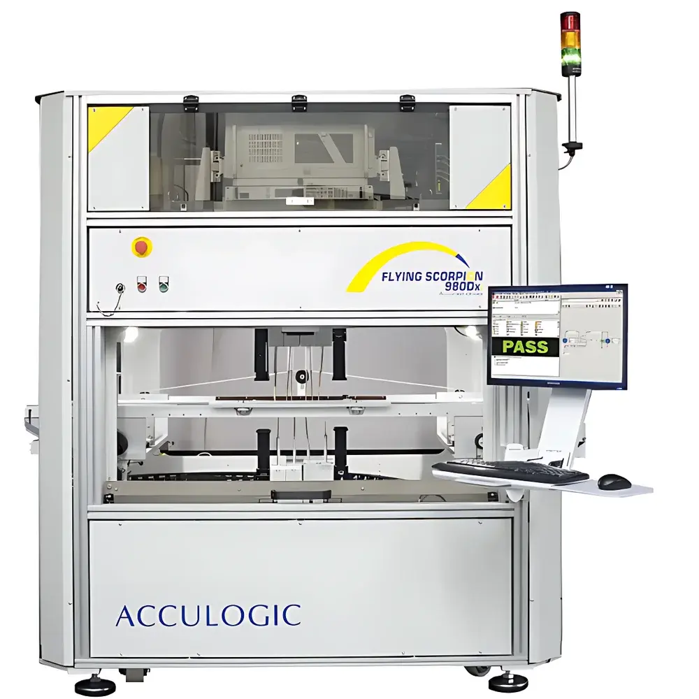
Acculogic FLS980 Flying Probe Test System
| Brand | Acculogic |
|---|---|
| Origin | Canada |
| Model | FLS980 |
| Configuration | Dual-Sided, Closed-Loop, Up to 22 Probes |
| Minimum Step Resolution | 1 µm |
| Positioning Repeatability | ±10 µm |
| Programmable Probe Tilt | ±6° |
| Max PCB Size | 813 × 965 mm (32″ × 38″) |
| Max Component Height | 85 mm |
| Max Probe Tip Radius | 50–500 µm |
| Analog Measurement Speed | Up to 1000 measurements/sec |
| 4-Wire Capability | Full per probe |
| Test Channel Count | Up to 128 non-multiplexed channels |
| Warpage Compensation | LaserScan + High-Resolution Vision |
| Compliance | Supports GLP/GMP audit trails, ASTM F2622 (for electronic assembly test systems), ISO/IEC 17025 traceability frameworks |
Overview
The Acculogic FLS980 Flying Probe Test System is a high-precision, dual-sided, closed-loop automated test platform engineered for functional and parametric validation of modern printed circuit assemblies—particularly those with ultra-fine-pitch components (down to 01005), high-density interconnects, and chip-scale packaging. Unlike traditional in-circuit testers requiring dedicated fixtures, the FLS980 employs dynamically positioned flying probes guided by real-time vision-based registration and laser-assisted warpage mapping. Its core architecture integrates linear motor-driven shuttles with independently programmable probe modules, enabling sub-10 µm positional repeatability across X, Y, and Z axes—even on boards exhibiting thermal or mechanical deformation up to 0.5 mm. The system operates on the principle of contact-based electrical interrogation: each probe establishes physical contact with test points while simultaneously delivering stimulus signals and acquiring response data via synchronized analog/digital measurement circuits. This approach supports both static parametric testing (e.g., resistance, capacitance, diode forward voltage) and dynamic functional verification—including powered-up device characterization and boundary-scan (IEEE 1149.x) execution—within a single platform.
Key Features
- Dual-sided probing architecture with up to 22 independently controlled flying probes (top and bottom combined), enabling full coverage of complex multilayer boards without manual reorientation.
- Closed-loop linear motor shuttles with AccuFast™ motion control: 1 µm minimum step resolution and ±10 µm positioning repeatability under industrial environmental conditions (20–25°C, <60% RH).
- Programmable probe tilt mechanism: ±6° angular adjustment per module, allowing optimized contact geometry for low-profile components and mitigating slippage-induced pad damage.
- Integrated high-resolution reference camera (5 MP, telecentric optics) and calibrated LED illumination for fiducial detection with sub-pixel accuracy; compensates for board translation, rotation, and scaling prior to probing.
- LaserScan™ 3D topography mapping subsystem: Captures Z-axis warpage profiles across the entire PCB surface (up to 813 × 965 mm), feeding real-time Z-offset corrections into the motion planner.
- Modular probe head options: APM 800 (fully programmable tilt, 0°–+6°), BPM 700 (+6° fixed tilt), and VPM 600 (vertical-only, 0°); all support interchangeable tip geometries (conical, cup, dome) and radii from 50 µm to 500 µm.
- High-speed analog measurement engine: 1000 measurements/sec maximum rate, full 4-wire Kelvin capability per probe pair, and configurable 2-wire/4-wire/quasi-4-wire modes for optimal signal integrity.
Sample Compatibility & Compliance
The FLS980 accommodates rigid, flex-rigid, and HDI PCBs ranging from prototype to high-mix production volumes. It supports components with standoff heights up to 85 mm and target pads as small as 100 µm in diameter. Board thickness tolerance spans 0.4 mm to 6.4 mm, with clamping force adjustable to prevent warpage-induced stress during probing. From a regulatory standpoint, the system’s software architecture—Integrator™—supports ALCOA+ principles for data integrity: attributable, legible, contemporaneous, original, accurate, complete, consistent, enduring, and available. Audit trail logging complies with FDA 21 CFR Part 11 requirements for electronic records and signatures when configured with user authentication and role-based access controls. Test methods align with ASTM F2622 (Standard Guide for Electrical Testing of Printed Wiring Boards) and IEC 61188-6 (Test Methods for Interconnection Structures), and measurement traceability follows ISO/IEC 17025 guidelines through NIST-traceable calibration protocols for voltage, current, resistance, and capacitance channels.
Software & Data Management
Integrator™ is the proprietary, Windows-based control and analysis suite that orchestrates motion planning, image processing, electrical measurement sequencing, and result aggregation. Its modular design separates hardware abstraction layers from test logic, enabling seamless integration with factory MES and PLM systems via OPC UA and RESTful APIs. The software includes NetScan™—a topology-aware netlist analysis engine that reduces test time by eliminating redundant shorts checks—and JTAG Navigator™ for IEEE 1149.1/1149.4/1149.6 boundary-scan test program generation directly from BSDL and SVF files. All measurement data is stored in structured SQLite databases with configurable retention policies; raw waveforms, pass/fail flags, statistical summaries (Cp/Cpk), and annotated optical images are exportable in CSV, PDF, and XML formats. Version-controlled test programs support rollback, comparative analysis, and change impact assessment across product revisions.
Applications
- Low-volume, high-mix electronics manufacturing: Eliminates fixture development lead time and cost for prototypes and engineering change orders.
- Failure analysis labs: Enables precise point-to-point continuity tracing, component-level parametric validation, and powered functional diagnostics on suspect assemblies.
- Aerospace and medical electronics: Supports DO-254/DO-178C and IEC 62304-compliant test documentation packages, including traceability matrices linking test cases to requirements.
- Contract manufacturers: Facilitates rapid line qualification and process capability studies (e.g., solder joint integrity, component placement accuracy) without dedicated ICT infrastructure.
- Reverse engineering and legacy board support: Optical recognition and adaptive probing enable test program generation from bare-board scans and schematic fragments.
FAQ
What is the smallest pad size the FLS980 can reliably contact?
The system achieves repeatable contact on pads as small as 100 µm in diameter using 50 µm-radius conical tips and ±6° tilt compensation—validated per IPC-A-610 Class 3 criteria.
Does the FLS980 support powered functional testing?
Yes. Integrated voltage regulation modules deliver programmable DC bias (±24 V, 2 A max) and AC stimulus (up to 1 MHz) for active device characterization, including LDO regulation, op-amp gain/phase, and switching regulator efficiency.
How does the system handle board warpage during probing?
LaserScan™ generates a full 3D height map prior to test execution; the motion controller applies dynamic Z-axis offsets to each probe trajectory, maintaining orthogonal contact force across warped surfaces.
Can test programs be migrated from legacy ICT platforms?
NetScan™ accepts industry-standard netlists (IPC-D-356, ODB++, Gerber X2) and supports automated conversion of fixture-based test steps into flying probe equivalents—including virtual short detection and path optimization.
Is remote monitoring and diagnostics supported?
Integrator™ includes embedded web server functionality for real-time status dashboards, alarm notifications via SMTP/SNMP, and secure remote desktop access for Tier-2 technical support—compliant with ISO/IEC 27001 network security baselines.


