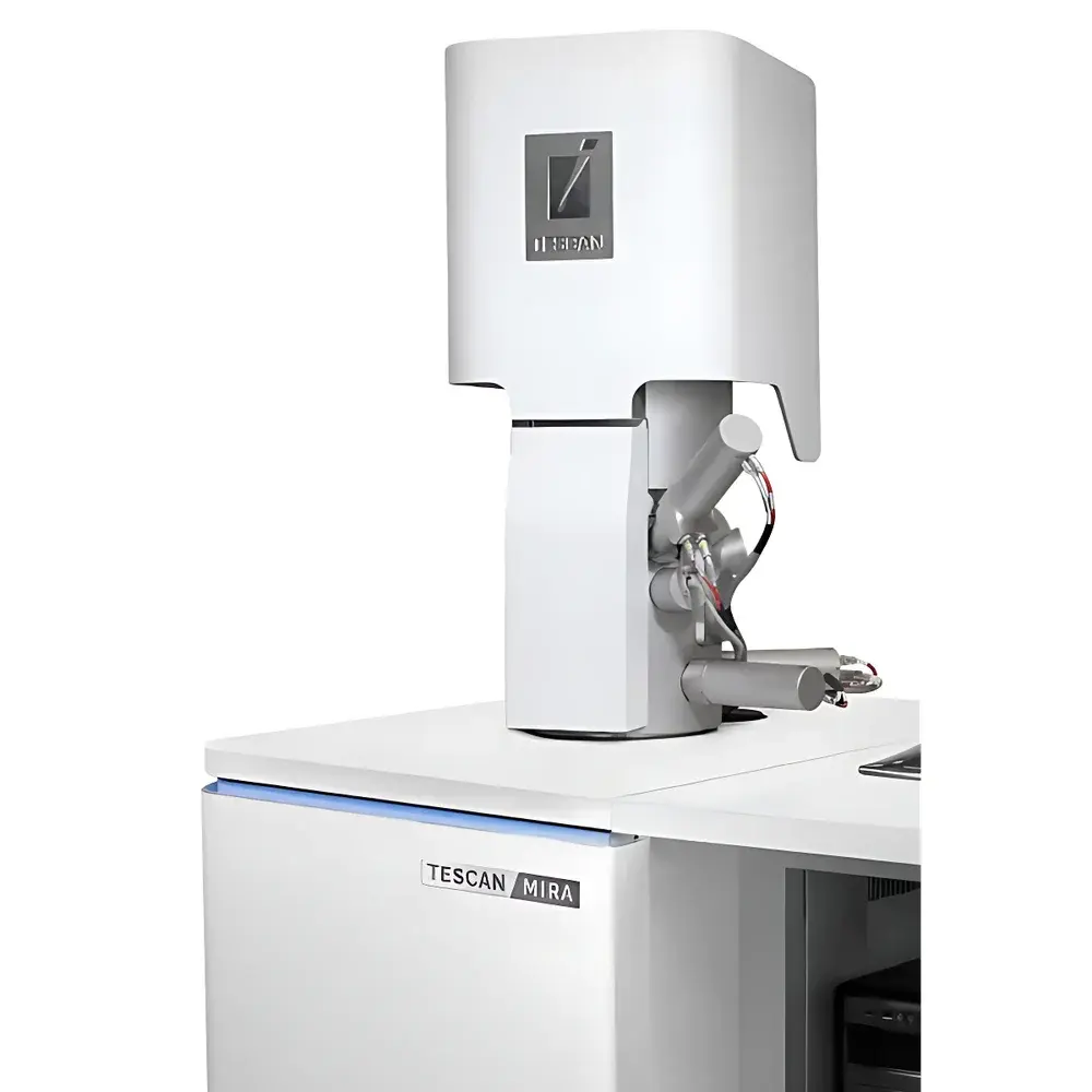
TESCAN MIRA Field Emission Scanning Electron Microscope
| Brand | TESCAN |
|---|---|
| Origin | Czech Republic |
| Model | TESCAN MIRA |
| Instrument Type | Floor-standing SEM |
| Electron Gun | Schottky Field Emission |
| Secondary Electron Resolution | 1.0 nm @ 30 kV |
| Magnification Range | 2× to 1,000,000× |
| Accelerating Voltage | 200 V – 30 kV (down to 50 V in deceleration mode) |
| Backscattered Electron Resolution | 2.0 nm @ 30 kV |
Overview
The TESCAN MIRA is a fourth-generation field emission scanning electron microscope (FE-SEM) engineered for high-resolution imaging, quantitative microanalysis, and robust routine operation in industrial quality control and academic research laboratories. It employs a high-brightness Schottky thermal field emission electron source, delivering stable probe current and exceptional signal-to-noise ratio across a wide accelerating voltage range (50 V–30 kV). Its optical architecture is based on a lens-free beam path design—enabled by TESCAN’s proprietary In-flight Beam Tracing™ technology—which eliminates traditional aperture constraints and allows real-time optimization of beam convergence, working distance, and stigmation without manual intervention. This architecture supports simultaneous high-resolution secondary electron (SE) and backscattered electron (BSE) imaging, as well as integrated energy-dispersive X-ray spectroscopy (EDS) analysis—all within a unified software interface.
Key Features
- Fully integrated TESCAN Essence™ EDS platform: Enables concurrent SEM imaging and live elemental mapping without switching applications or windows—critical for rapid failure analysis and process validation.
- Wide Field Optics™: Delivers true 2× minimum magnification with full-field navigation capability, eliminating the need for auxiliary optical cameras while maintaining sub-nanometer resolution at high magnifications.
- SingleVac™ mode: Allows direct imaging of non-conductive or beam-sensitive specimens—including polymers, biological tissues, and uncoated ceramics—without sputter coating or charge compensation hardware.
- In-flight Beam Tracing™: Dynamically monitors and corrects beam trajectory during stage movement and focus adjustment, ensuring consistent image quality and analytical reproducibility across variable working distances and tilt angles.
- Essence™ 3D collision avoidance model: Uses real-time spatial registration of detector positions, pole piece geometry, and stage kinematics to prevent mechanical interference during automated acquisition sequences.
- Modular detector architecture: Supports in-column SE and BSE detectors, decelerated beam imaging for enhanced surface sensitivity, and optional accessories including cryo-stages, cathodoluminescence (CL) detectors, and liquid nitrogen-cooled BSE detectors.
Sample Compatibility & Compliance
The MIRA accommodates samples up to 200 mm in diameter and 100 mm in height in standard configuration, with extended chamber options available for larger or irregularly shaped specimens. Its vacuum system features differential pumping stages optimized for both high-vacuum (<1×10⁻⁷ Pa) and low-vacuum (up to 100 Pa) operation—enabling analysis of hydrated, outgassing, or insulating materials under controlled partial pressure. The instrument complies with IEC 61000-6-2 (EMC immunity) and IEC 61000-6-4 (EMC emissions), and its software architecture supports audit trails, user access levels, and electronic signatures per FDA 21 CFR Part 11 requirements when deployed in regulated environments (e.g., pharmaceutical QC or medical device R&D).
Software & Data Management
TESCAN Essence™ is a modular, scriptable, and standards-compliant software suite built on a Qt-based framework. It provides synchronized control of imaging, stage navigation, EDS acquisition, and spectral quantification—all accessible from a single tabbed interface. Data files are stored in vendor-neutral HDF5 format with embedded metadata (including acquisition parameters, calibration history, and detector geometry), facilitating long-term archival and third-party processing via Python-based tools (e.g., HyperSpy, DTSA-II). Batch processing workflows support automated particle analysis, line scans, and hyperspectral cube generation, with export options compliant with ASTM E1508 (quantitative EDS microanalysis) and ISO 16700 (SEM-EDS elemental mapping protocols).
Applications
- Semiconductor & Microelectronics: Cross-sectional inspection of TSVs, solder joint integrity assessment, intermetallic phase identification in BGA packages, and nanoscale defect localization in advanced nodes.
- Materials Science: Grain boundary characterization in high-entropy alloys, porosity quantification in thermal barrier coatings, fiber-matrix interface analysis in CFRP composites, and phase distribution mapping in multiphase ceramics.
- Life Sciences: Ultrastructural morphology of freeze-fractured membranes, collagen fibril orientation in decellularized scaffolds, nanoparticle internalization in macrophages, and elemental co-localization in mineralized bone tissue.
- Geosciences & Environmental Analysis: Mineral phase discrimination in polished thin sections, microplastic identification in sediment cores, heavy metal speciation in fly ash particles, and pore-network modeling in shale reservoir rocks.
FAQ
What vacuum modes does the MIRA support?
The MIRA operates in high vacuum (HV), low vacuum (LV), and SingleVac™ modes—each selectable via software without hardware reconfiguration.
Can EDS analysis be performed simultaneously with SE imaging?
Yes. Essence™ enables real-time spectrum acquisition synchronized with frame-by-frame image capture, supporting dynamic compositional tracking during in-situ experiments.
Is the system compatible with automated stage mapping and scripting?
Yes. The Essence™ API supports Python-based automation for batch acquisition, region-of-interest (ROI) definition, and conditional triggering of EDS collection based on intensity thresholds.
What level of training is required to operate the MIRA independently?
Operators with basic SEM knowledge can perform routine imaging and EDS point analysis after a two-day hands-on workshop; advanced correlative workflows require additional application-specific training.
How is beam damage minimized for sensitive biological samples?
Through combined use of SingleVac™ mode, low-kV deceleration optics (down to 50 V landing energy), dwell time optimization, and optional beam blanking synchronization with stage motion.


