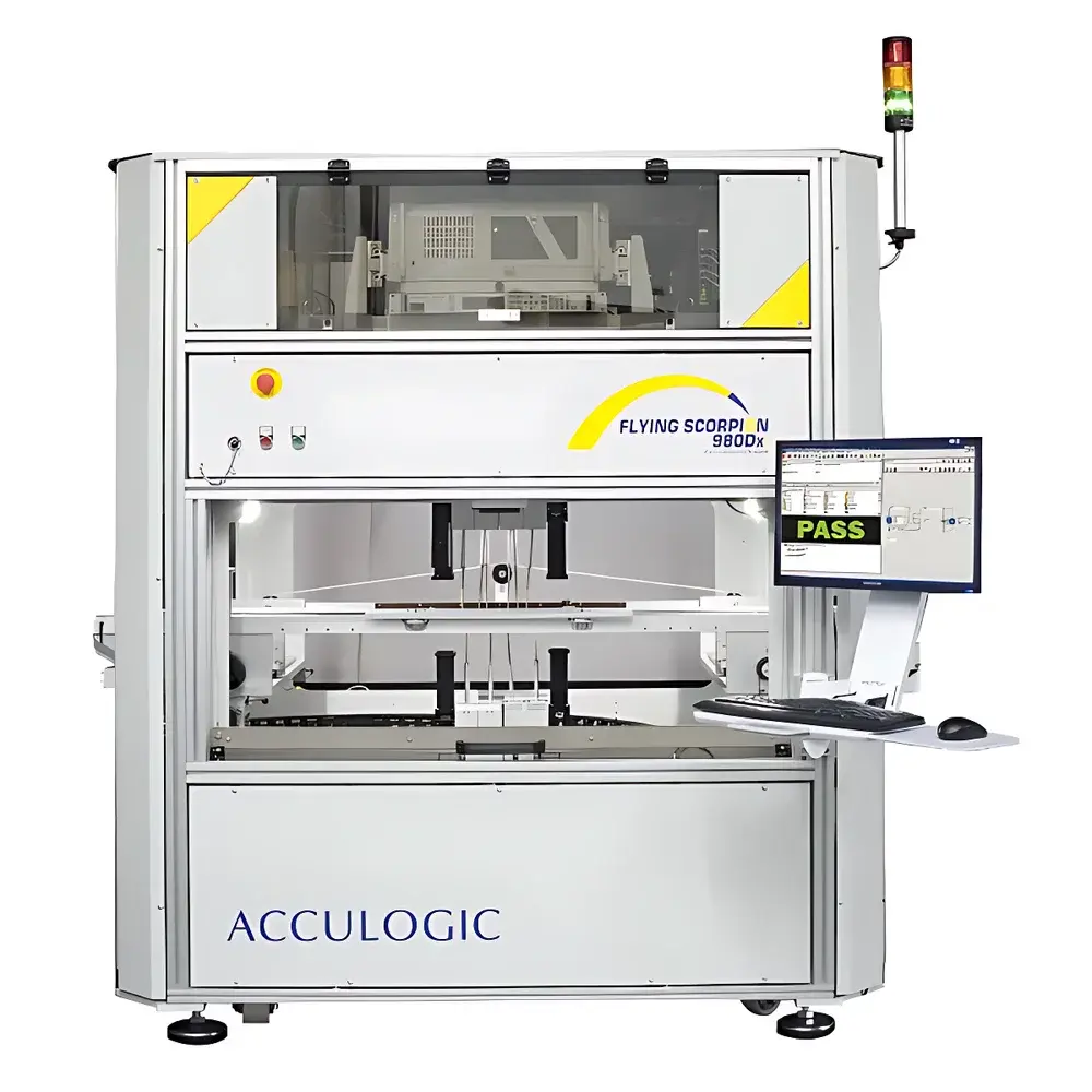
Acculogic FLS980 Series Flying Probe Tester
| Brand | Acculogic |
|---|---|
| Origin | Canada |
| Manufacturer Type | Authorized Distributor |
| Product Origin | Imported |
| Model | ACCULOGIC FLS980 Series |
| Pricing | Upon Request |
Overview
The Acculogic FLS980 Series Flying Probe Tester is a high-precision, dual-sided, closed-loop flying probe test system engineered for advanced functional and electrical validation of modern printed circuit assemblies (PCBAs). Designed to address the evolving challenges of miniaturization—including 01005 passives, fine-pitch BGAs, chip-scale packages (CSP), and board-level integration—the FLS980 employs a hybrid motion architecture combining linear motor-driven shuttles with independently programmable probe modules. Its core measurement principle relies on real-time coordinated motion control, vision-guided calibration, and laser-based board warpage compensation to achieve sub-10 µm positional repeatability across X, Y, and Z axes. Unlike open-loop systems, the FLS980 implements full闭环 feedback at both shuttle and probe module levels, eliminating mechanical hysteresis and ensuring traceable metrological stability in production environments. The system supports live power-on functional testing up to GHz-frequency ranges, enabling verification of high-speed digital interfaces, analog signal integrity, mixed-signal behavior, and boundary-scan (IEEE 1149.x) compliance—making it suitable for R&D validation, NPI support, and low-to-medium volume manufacturing where fixtureless flexibility is critical.
Key Features
- Dual-sided probing architecture supporting up to 22 independently controlled flying probes (top and bottom combined)
- AccuFast™ closed-loop linear motor shuttle system with 1 µm minimum step resolution and ±10 µm positioning repeatability
- Programmable probe tilt capability from –6° to +6° per module, enabling adaptive contact geometry for warped or uneven boards
- High-resolution reference camera with precision illumination and sub-pixel centroid detection for fiducial recognition and board offset compensation
- LaserScan™ 3D topography mapping for real-time board warpage quantification and Z-axis correction during probing
- 4-wire Kelvin measurement capability across all 22 probes, supporting resistance, capacitance, inductance, diode, transistor, and IC-level parametric testing
- Integrated NetScan™ and JTAG/Boundary Scan test engines compliant with IEEE 1149.1/1149.4/1149.6 standards
- Configurable probe module types: APM-800 (fully programmable tilt), BPM-700 (fixed +6° tilt), and VPM-600 (vertical 0°)
- Probe tip radius range: 50–500 µm; selectable tip geometries including conical, cup, and dome profiles
- Maximum component height clearance: 85 mm; maximum probe travel height: 45 mm
Sample Compatibility & Compliance
The FLS980 accommodates PCBs up to 813 × 965 mm (32″ × 38″), supporting rigid, flex-rigid, and HDI substrates with feature sizes down to 100 µm. Its adaptive probing strategy enables reliable contact with ultra-fine-pitch components (e.g., 0.3 mm pitch QFNs, 01005 passives) without pad damage or via skid. The system complies with IPC-A-610 Class 2 and Class 3 visual inspection guidelines for contact verification, and its measurement firmware supports audit-ready data logging aligned with ISO/IEC 17025 requirements for calibration traceability. For regulated industries, the Integrator™ control software provides configurable user roles, electronic signatures, and audit trail functionality compatible with FDA 21 CFR Part 11 and GLP/GMP documentation workflows.
Software & Data Management
The Integrator™ platform serves as the unified control, programming, and diagnostics environment for the FLS980. It features an intuitive graphical test development interface supporting drag-and-drop test sequencing, automatic netlist import (IPC-D-356, ODB++, Gerber), and intelligent probe path optimization. All measurements are timestamped and logged with full metadata—including probe ID, XYZ coordinates, tilt angle, contact force estimate, and environmental conditions. Export formats include CSV, XML, and industry-standard STDF (Semiconductor Test Data Format) for integration with MES and SPC systems. Firmware updates and configuration backups are managed via secure HTTPS-based remote deployment, and system health monitoring includes real-time shuttle encoder diagnostics, probe wear tracking, and thermal drift compensation logs.
Applications
- Fixtureless functional validation of prototype and low-volume PCBAs in electronics design centers
- Failure analysis and root cause investigation of solder joint defects, opens, shorts, and parametric drift
- Reverse engineering support through automated net identification, component footprint mapping, and schematic reconstruction
- Verification of embedded test access mechanisms (e.g., JTAG chains, BSCAN controllers) prior to system-level integration
- Post-rework verification following reballing, component replacement, or conformal coating removal
- Qualification testing of new substrate technologies, including embedded passives and heterogeneous integration platforms
- Supplier qualification audits requiring traceable, repeatable electrical test evidence without custom fixtures
FAQ
What is the maximum PCB size supported by the FLS980 Series?
The system accommodates boards up to 813 mm × 965 mm (32″ × 38″), with optional edge-clamp configurations for oversized or irregularly shaped assemblies.
Does the FLS980 support powered functional testing?
Yes—it delivers live power-on testing capabilities up to GHz frequency ranges, including voltage regulation verification, op-amp gain/phase response, and high-speed serial link eye diagram sampling when integrated with external digitizers.
How does the system compensate for board warpage during probing?
LaserScan™ acquires a full 3D surface map prior to test execution; this data is fused with real-time camera-based fiducial tracking to dynamically adjust probe Z-height and tilt angles across the entire test area.
Can the FLS980 perform 4-wire resistance measurements?
Yes—all 22 probes support true 4-wire (Kelvin) measurements simultaneously, with dedicated force/sense pairs assignable per test step to eliminate lead resistance errors.
Is boundary scan (JTAG) testing integrated into the platform?
Yes—the system includes native IEEE 1149.1/1149.4/1149.6-compliant boundary scan engine with auto-chain discovery, instruction register programming, and BSDL parsing capabilities.


