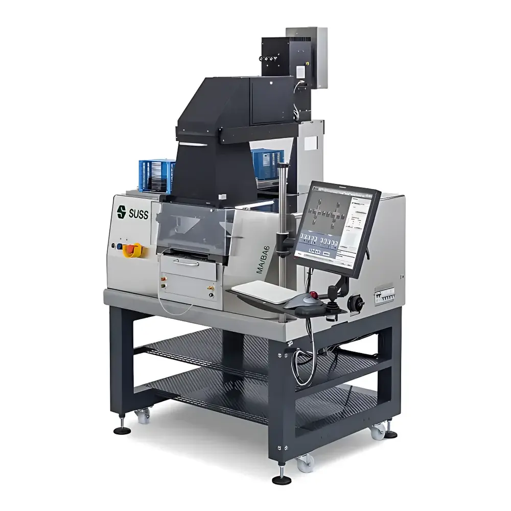
SUSS MA/BA Gen4 Semi-Automated Mask Aligner and Nanoimprint Lithography System
| Brand | SUSS MicroTec |
|---|---|
| Country of Origin | Germany |
| Model | MA/BA Gen4 |
| Type | Semi-Automated Mask Aligner & Thermal/Nanoimprint Lithography Platform |
| Application Scope | R&D, Pilot Production, High-Volume Prototyping |
| Compliance | ISO 9001 Certified Manufacturing, CE Marked, Compatible with ISO 14644-1 Class 5 Cleanroom Integration |
| Optical System | MO Exposure Optics® with Telecentric Illumination |
| Alignment Modes | Top-Side, Bottom-Side, IR Alignment |
| Optional Alignment Accuracy | ≤ 0.5 µm (with DirectAlign®) |
| Resolution | Down to 0.8 µm (hard/soft/vacuum contact mode) |
| Substrate Compatibility | 100–200 mm wafers, reticles, glass, quartz, SiC, GaAs, flexible substrates |
| Automation Level | Semi-Automated with SMILE™ Process Integration Framework |
| Software | LITHOGRAPH® v5.x with Audit Trail, User Role Management, Recipe Versioning, and GLP/GMP-Ready Data Logging |
Overview
The SUSS MA/BA Gen4 Semi-Automated Mask Aligner and Nanoimprint Lithography System is an integrated platform engineered for high-precision photolithography and thermal nanoimprint lithography (NIL) in semiconductor R&D, mask manufacturing, MEMS/NEMS development, advanced packaging, and micro-optics prototyping. Built upon SUSS MicroTec’s decades-long heritage in contact lithography, the Gen4 architecture combines proven optical mechanics with next-generation human-centered automation. Its core measurement and process principle relies on proximity or vacuum contact alignment between a photomask (or imprint stamp) and substrate under controlled illumination—enabling pattern transfer via UV exposure (for photoresist processing) or thermomechanical deformation (for polymer-based NIL). Unlike fully automated cluster tools, the MA/BA Gen4 maintains operator oversight while minimizing manual intervention through guided workflows, ergonomic interface design, and real-time alignment feedback—making it ideal for low-to-medium volume production environments where flexibility, traceability, and process reproducibility are prioritized over throughput alone.
Key Features
- MO Exposure Optics® with telecentric illumination delivering ≥95% illumination uniformity across full-field exposure (up to 200 mm), critical for consistent resist crosslinking and NIL residual layer control.
- Triple-mode alignment system: top-side visible-light, bottom-side transmitted-light, and infrared (IR) alignment—supporting opaque substrates, multi-layer stacks, and embedded alignment marks.
- DirectAlign® optional module enabling real-time image correlation and sub-micron overlay registration (≤0.5 µm @ 3σ), validated per ISO 10110-7 and ASTM F2609 standards.
- Modular mechanical architecture accommodating interchangeable exposure heads, imprint modules (thermal or UV-NIL), and vacuum chucks for rigid/flexible substrates (Si, quartz, glass, polyimide, metal foils).
- SMILE™ (Smart Modular Integration & Lithography Environment) framework allowing seamless integration of external metrology tools, environmental sensors, and inline process monitoring systems via SECS/GEM protocol.
- Ergonomic recipe editor with drag-and-drop parameter sequencing, context-sensitive help, and syntax validation—reducing operator training time by up to 40% compared to legacy aligners.
Sample Compatibility & Compliance
The MA/BA Gen4 supports substrates ranging from 100 mm silicon wafers to 200 mm reticles, including compound semiconductors (GaAs, InP, SiC), fused silica masks, and non-planar polymer films. Its vacuum chuck design ensures flatness control within ±0.5 µm across 150 mm diameter, meeting requirements for high-resolution patterning in AR waveguide fabrication and photonic integrated circuit (PIC) prototyping. The system complies with EU Machinery Directive 2006/42/EC, Electromagnetic Compatibility Directive 2014/30/EU, and carries CE marking. All software functions—including user authentication, audit trail logging, electronic signatures, and data export—conform to FDA 21 CFR Part 11 and EU Annex 11 expectations for regulated environments. Full documentation packages (IQ/OQ/PQ templates, calibration certificates, and maintenance logs) are provided to support GLP and GMP audits.
Software & Data Management
LITHOGRAPH® v5.x serves as the unified control and data management suite, featuring role-based access control (RBAC) with five-tier permission levels (Operator, Technician, Engineer, QA, Admin). Every exposure or imprint event is timestamped, logged with full parameter snapshots (intensity, dose, focus offset, vacuum pressure, temperature ramp rate), and linked to associated mask ID, substrate lot number, and operator credentials. Data retention policies support configurable archiving (local NAS or cloud S3-compatible endpoints), with SHA-256 hashing for integrity verification. Export formats include CSV, XML, and HDF5—compatible with JMP, MATLAB, and industry-standard MES platforms. Optional LIMS integration enables automatic job dispatching and yield reporting aligned with SEMI E10 and E142 standards.
Applications
The MA/BA Gen4 delivers repeatable performance across diverse use cases: mask writing verification and repair qualification; MEMS device patterning (e.g., inertial sensors, RF-MEMS switches); fan-out wafer-level packaging (FOWLP) redistribution layer (RDL) definition; plasmonic nanostructure replication for biosensing; micro-lens array fabrication for LiDAR optics; and hybrid integration of III-V devices onto silicon photonics platforms. Its dual-capability architecture eliminates the need for separate photolithography and NIL tools during early-stage process development—accelerating technology transfer from lab to pilot line while preserving metrological continuity across toolsets.
FAQ
What substrate sizes does the MA/BA Gen4 support?
Standard configurations accommodate 100 mm, 150 mm, and 200 mm circular substrates; rectangular reticles up to 152 × 152 mm are supported with optional fixture kits.
Is the system compatible with UV-NIL and thermal NIL processes?
Yes—the MA/BA Gen4 Pro variant includes dual-source capability: mercury-xenon broadband UV (350–450 nm) for photoresist exposure and independently controlled heated stamp stage (up to 200 °C) for thermal imprinting.
Can alignment be performed through opaque layers?
Yes—using integrated IR alignment optics (1310 nm wavelength), the system detects alignment marks beneath metal layers or thick dielectrics without requiring backside thinning.
How is process traceability ensured?
Every run generates a cryptographically signed log file containing raw sensor data, operator actions, environmental conditions, and final alignment metrics—fully compliant with ISO/IEC 17025 and IATF 16949 record retention requirements.
Does SUSS provide application support for new material systems?
Yes—SUSS Application Labs offer joint development programs for novel resists (e.g., metal-organic frameworks, hybrid sol-gels), custom stamp fabrication, and process window optimization using Design of Experiments (DoE) methodology.


