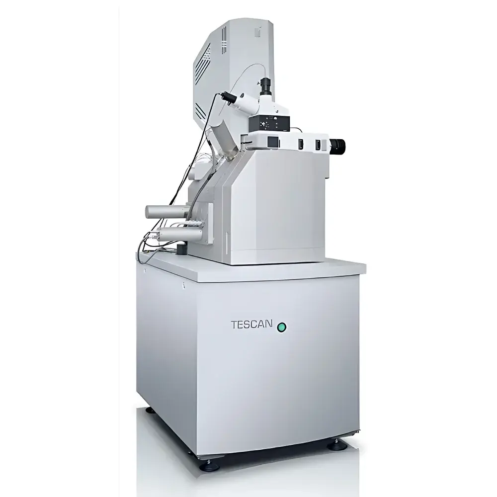
TESCAN RISE Integrated SEM-Raman Microscope
| Brand | TESCAN |
|---|---|
| Origin | Czech Republic |
| Electron Gun Type | Cold Field Emission |
| Secondary Electron Resolution | 1.0 nm @ 15 kV |
| Accelerating Voltage Range | 0.2–30 kV |
| Backscattered Electron Resolution | 1.0 nm @ 15 kV |
Overview
The TESCAN RISE Integrated SEM-Raman Microscope represents a paradigm shift in correlative microanalysis by unifying high-resolution scanning electron microscopy (SEM) with confocal Raman spectroscopy within a single, co-registered platform. Unlike conventional sequential or offline correlation approaches, the RISE system enables true spatial and temporal synchronization: electron-induced topographic, compositional (via BSE/EDS), and crystallographic data are acquired *in situ* alongside molecular vibrational signatures—without sample relocation, stage repositioning, or vacuum break. This integration is grounded in precise mechanical alignment of the electron optical column and the Raman optical path, ensuring sub-100 nm registration accuracy between SEM images and Raman spectral maps. Engineered for materials science laboratories requiring nanoscale structural–chemical correlation, the RISE platform operates under high-vacuum conditions compatible with cold field emission (CFE) electron sources, delivering stable beam current and exceptional signal-to-noise ratio across the full accelerating voltage range (0.2–30 kV). Its design adheres to fundamental principles of electron–photon synergy: secondary electrons (SE) reveal surface morphology at ≤1.0 nm resolution (at 15 kV), while backscattered electrons (BSE) provide atomic number contrast; simultaneously, the integrated confocal Raman module collects spectrally resolved vibrational data with diffraction-limited spatial resolution (~0.5 µm lateral, ~1–2 µm axial), enabling chemical identification, phase mapping, stress quantification, crystallinity assessment, and layer-thickness determination in layered 2D materials.
Key Features
- Co-aligned, dual-beam architecture: CFE-SEM column and confocal Raman microscope share a common sample coordinate system with <100 nm registration fidelity
- Cold field emission electron source for high brightness, long-term stability, and low energy spread—critical for high-resolution imaging and low-kV surface-sensitive analysis
- Full voltage tunability (0.2–30 kV) supporting both surface-sensitive low-voltage imaging and deep-penetration high-energy characterization
- Integrated motorized XYZ-stage with sub-nanometer repeatability and software-synchronized navigation between SEM and Raman acquisition zones
- Automated spectral acquisition grid: user-defined ROI mapping with pixel-by-pixel Raman spectra (e.g., 128×128 spectral map) overlaid directly onto SEM reference frames
- Real-time spectral preview and live Raman intensity mapping during SEM navigation—no post-hoc image registration required
- Optimized optical coupling: high-throughput transmission optics and notch-filtered detection minimize laser-induced damage and maximize signal collection efficiency
Sample Compatibility & Compliance
The RISE platform accommodates standard SEM-compatible specimens—including conductive and non-conductive bulk solids, polished cross-sections, thin films, powders on stubs, and biological samples (with appropriate coating)—without compromising Raman signal integrity. Non-conductive samples may be analyzed in low-vacuum mode (optional) or with ultra-thin carbon coating (<2 nm), preserving molecular fingerprinting capability. The system complies with IEC 61000-6-3 (EMC emissions) and IEC 61000-6-2 (immunity), and its vacuum interlock architecture meets ISO 14644-1 Class 5 cleanroom operational standards. For regulated environments, optional audit-trail-enabled software supports 21 CFR Part 11 compliance (electronic signatures, secure user roles, immutable acquisition logs), facilitating GLP/GMP-aligned workflows in pharmaceutical excipient characterization, medical device material verification, and geological reference material certification.
Software & Data Management
TESCAN’s Unified Platform (UP) software provides a single GUI for instrument control, acquisition orchestration, and multimodal data fusion. It natively supports hierarchical data storage in HDF5 format, preserving metadata (e.g., kV, working distance, laser power, grating, objective magnification) with each spectrum and image. Advanced correlation tools include: (i) vector-based ROI transfer from SEM to Raman grid; (ii) false-color Raman parameter mapping (e.g., peak position for stress, FWHM for crystallinity, intensity ratio for layer count); (iii) multivariate statistical analysis (PCA, cluster analysis) applied directly to hyperspectral Raman cubes; and (iv) export to third-party packages (MATLAB, Python via h5py, Thermo Fisher Avizo) for custom modeling. All raw and processed datasets are timestamped, version-controlled, and exportable in FAIR-compliant formats (ISA-Tab, mzML-inspired schema).
Applications
- Carbon nanomaterials: Distinguishing monolayer vs. bilayer graphene via 2D-band intensity ratios; quantifying defect density (D/G ratio) and strain distribution across CVD-grown domains
- Mineralogy & geoscience: In situ differentiation of polymorphs (e.g., anatase vs. rutile TiO₂), fluid inclusion analysis, and metamorphic grade assessment via quartz Raman shifts
- Pharmaceuticals: Mapping API–excipient distribution in tablets; detecting polymorphic transitions induced by milling or humidity exposure
- Advanced polymers: Identifying phase-separated domains in block copolymers; correlating crystalline lamellae (SEM) with local crystallinity (Raman FWHM)
- Biomedical materials: Localizing drug-loaded nanoparticles within tissue sections; assessing collagen cross-linking state via amide I band deconvolution
- Jewelry & gemology: Non-destructive identification of natural vs. synthetic diamonds, HPHT-treated sapphires, and composite emeralds using characteristic lattice modes
FAQ
How is spatial correlation achieved without mechanical drift?
The RISE system uses a rigid, monolithic optical–electron column mount and real-time stage encoder feedback to maintain sub-100 nm positional fidelity across multi-hour acquisitions.
Can Raman analysis be performed under high vacuum?
Yes—the integrated Raman module operates fully inside the SEM chamber; laser delivery and signal collection occur through vacuum-compatible fused silica windows and reflective optics.
Is EDS data collected simultaneously with Raman?
No—EDS and Raman are acquired sequentially but co-registered; however, acquisition order is user-definable and synchronized via shared stage coordinates and time-stamped metadata.
What laser wavelengths are supported?
Standard configurations include 532 nm and 785 nm excitation; optional 638 nm and UV (325 nm) modules are available for resonance enhancement or reduced fluorescence interference.
Does the system support depth profiling?
Yes—confocal Raman enables optical sectioning; combined with SEM cross-section imaging, it allows 3D reconstruction of chemical gradients in layered structures (e.g., battery electrodes, coated implants).


