EMU IDWR Batch Wafer ID Reader
| Brand | EMU |
|---|---|
| Origin | UK |
| Manufacturer Type | Authorized Distributor |
| Product Category | Imported Equipment |
| Model | IDWR |
| Price Range | USD 14,000 – 72,000 (FOB) |
| Compatible Wafer Diameters | 75 mm, 100 mm, 125 mm, 150 mm, 200 mm |
| Throughput | 25 wafers per batch in ≤ 120 seconds (including cassette mapping, batch alignment, and full-surface ID reading) |
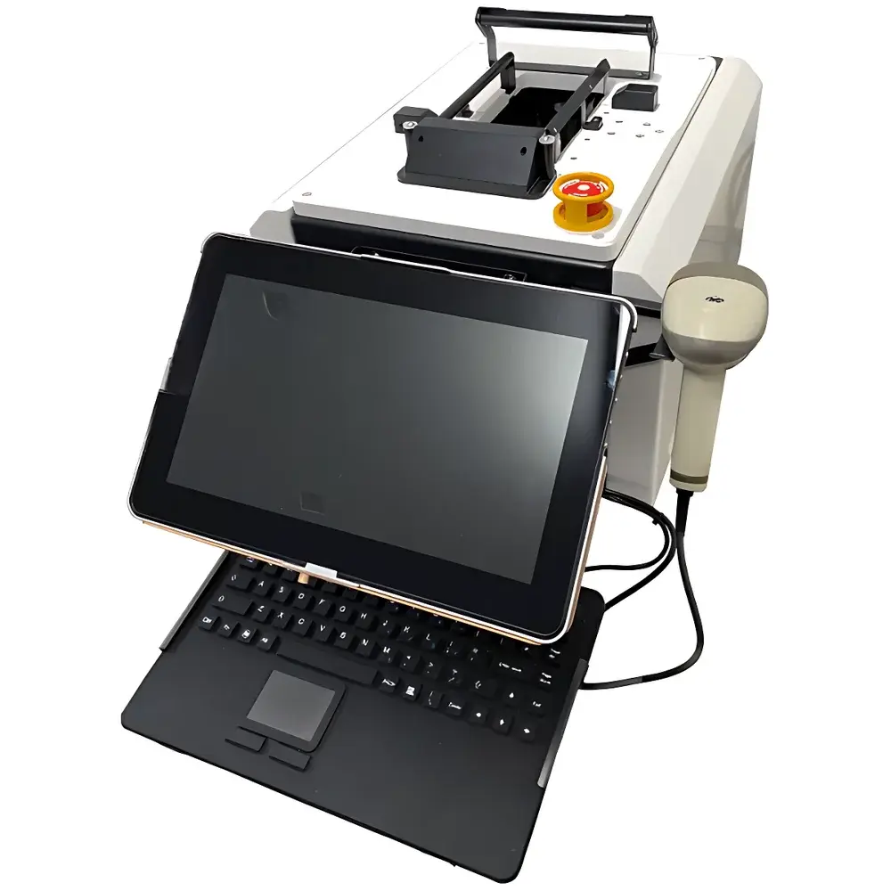
| Imaging System | Cognex In-Sight 1741 Smart Camera |
| Read Targets | Laser-etched marks and Data Matrix codes on wafer frontside and backside |
| Interface Protocols | RS-232, Ethernet, SECS/GEM compliant |
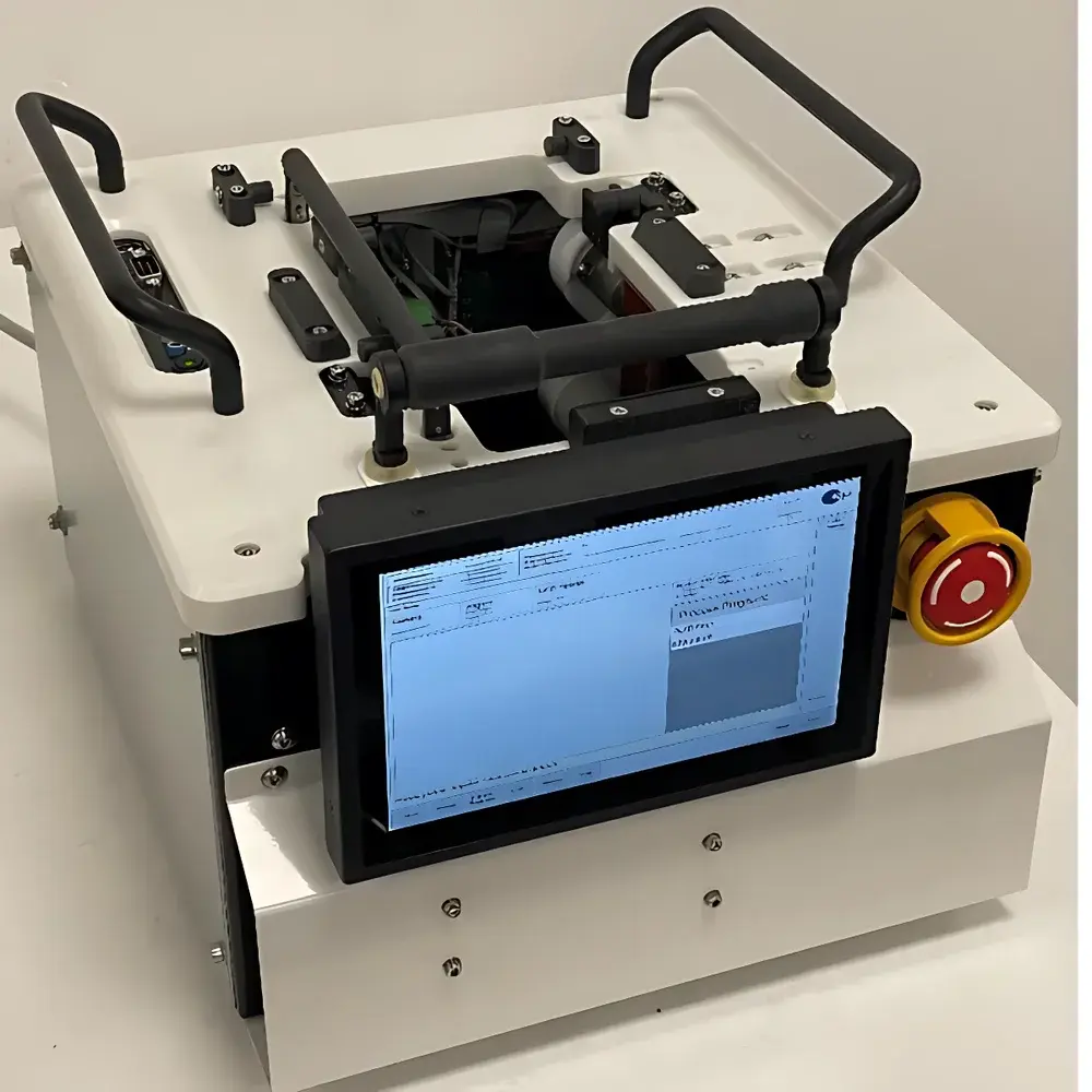
| User Interface | Integrated industrial touchscreen with recipe management and maintenance diagnostics |
Overview
The EMU IDWR Batch Wafer ID Reader is an engineered solution for high-throughput, non-contact identification and traceability verification of semiconductor wafers in front-end and backend manufacturing environments. Designed specifically for integration into automated wafer handling workflows—including sorters, testers, and load/unload stations—the IDWR operates on the principle of machine vision–based optical decoding, leveraging a calibrated Cognex In-Sight 1741 smart camera system to detect and decode laser-marked alphanumeric identifiers and ISO/IEC 16022-compliant Data Matrix symbols. Unlike single-wafer ID readers, the IDWR implements patented batch alignment technology that simultaneously references multiple wafers within a standard FOUP or open cassette, enabling consistent focal plane registration across variable wafer thicknesses and bow profiles. This architecture eliminates individual wafer centering steps, significantly reducing cycle time while maintaining sub-pixel positional repeatability (< ±2.5 µm at 200 mm). The system supports both frontside and backside reading—critical for fab-wide traceability where process history is encoded on the wafer back surface—and performs pre-read validation including cassette slot mapping and double-slot/dropped-wafer detection.
Key Features
- Patented batch alignment algorithm synchronizes optical focus and coordinate referencing across up to 25 wafers in a single cassette without mechanical repositioning.
- Cognex In-Sight 1741 vision engine with high dynamic range CMOS sensor, programmable illumination control, and embedded decoding firmware optimized for low-contrast laser marks and etched Data Matrix codes.
- Multi-diameter compatibility: validated operation across 75 mm through 200 mm wafers using field-replaceable stage adapters and auto-calibrated lens focus presets.
- SECS/GEM v2.0-compliant communication stack ensures seamless integration with factory host systems, supporting HSMS over TCP/IP and legacy RS-232 fallback modes.
- Industrial-grade touchscreen HMI with role-based access control (operator, engineer, admin), audit-trail-enabled recipe versioning, and real-time diagnostic logging.
- Pre-read cassette integrity check: automatically verifies slot occupancy, detects missing, double-loaded, or misaligned wafers prior to imaging—reducing downstream handling errors.
Sample Compatibility & Compliance
The IDWR accommodates standard SEMI-compliant wafer cassettes (e.g., 25-slot FOUPs, open carriers) and supports wafers with native oxide, SiN, SiO₂, or metalized surfaces. It reads identifiers applied via UV laser marking (≥ 20 µm feature size), fiber laser ablation (≥ 15 µm line width), and photolithographic Data Matrix patterns (minimum module size 30 µm). All optical paths are sealed against particulate ingress per ISO Class 5 cleanroom requirements. The system conforms to SEMI E10 (Definition and Measurement of Equipment Reliability and Availability), SEMI E30 (GEM Standard), and IEC 61000-6-2/6-4 for electromagnetic compatibility. Firmware and HMI software support audit trail generation per FDA 21 CFR Part 11 requirements when configured with network-authenticated user roles and electronic signature modules.
Software & Data Management
Firmware is field-upgradable via secure HTTPS interface; all configuration changes and read events are timestamped and stored locally in SQLite databases with configurable retention policies (default: 90 days). Decoded IDs are output in ASCII-encoded ASCII text format or JSON payloads, including wafer position index, read confidence score (0–100), orientation angle, and timestamp (UTC). Optional OPC UA server add-on enables direct publishing to MES/SCADA platforms. Data export supports CSV, XML, and SML formats compatible with FabLink XT, CIM300, and other industry-standard automation frameworks. Maintenance logs include camera health metrics (exposure drift, LED intensity decay), alignment calibration validity windows, and sensor temperature variance history.
Applications
- Front-end wafer sort: verifying lot/batch IDs prior to probe station loading and parametric testing.
- Backend traceability: confirming die-level test data linkage during final test handler integration.
- Reclaim and rework tracking: validating wafer identity after cleaning, repolishing, or mask rework cycles.
- Automated material movement: enabling closed-loop dispatch logic in AMHS-controlled fabs.
- Qualification of laser marking processes: quantifying decode success rate across wafer batches as part of process capability studies (Cp/Cpk).
FAQ
Does the IDWR require manual wafer centering before reading?
No. The patented batch alignment system uses fiducial-based coordinate transformation to register all wafers relative to the cassette frame, eliminating per-wafer centering steps.
Can it read Data Matrix codes on warped 200 mm wafers?
Yes. The system employs depth-aware focus stacking and adaptive thresholding to maintain decode reliability on wafers with up to 50 µm total indicator reading (TIR) bow.
Is SECS/GEM implementation certified by SEMI?
The IDWR’s GEM implementation has passed SEMI E30 conformance testing (certificate #GEM-2023-EMU-IDWR-0871) and supports HSMS-SS and HSMS-GS session modes.
What happens if a wafer is missing from its assigned slot?
The cassette mapping routine triggers a Level 2 alarm, halts further processing, and reports the affected slot index—preventing misattribution of IDs to incorrect wafers.
How often does the system require recalibration?
Optical alignment calibration is valid for 180 days under normal operating conditions (22 ± 3°C, <50% RH); automated self-check runs at startup and every 24 hours.
Related Products


