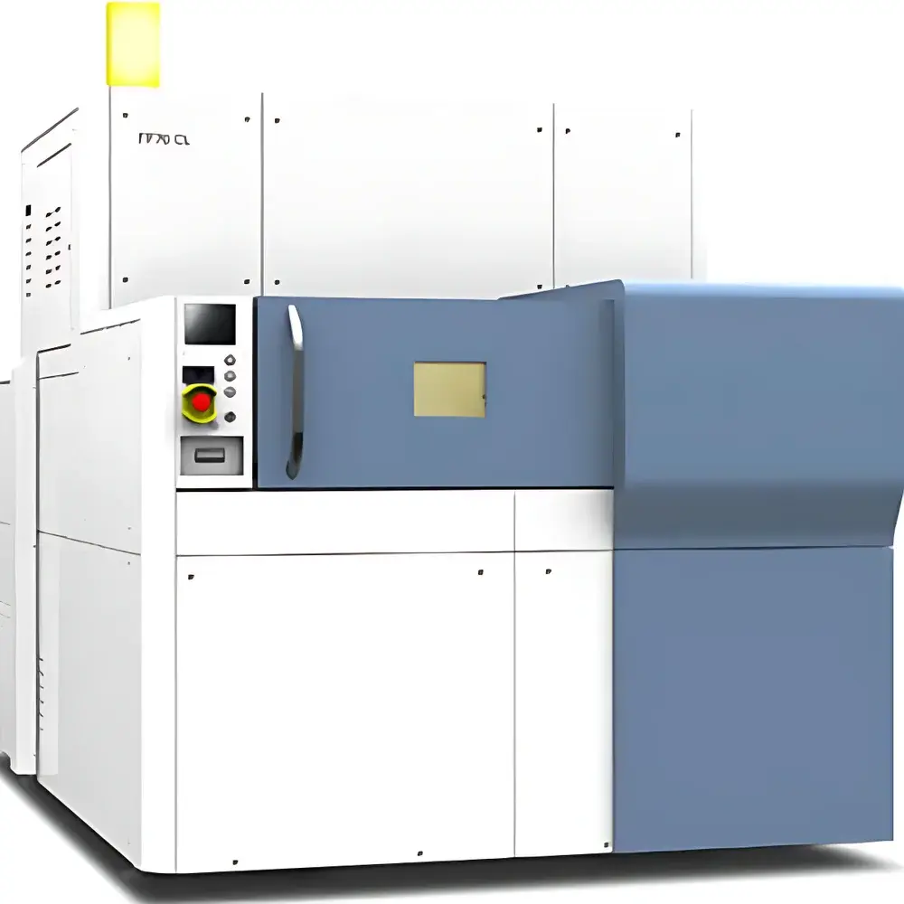
YXLON FF70 CL High-Resolution Industrial Micro-CT System
| Brand | YXLON |
|---|---|
| Origin | Germany |
| Model | FF70 CL |
| Detector Type | High-Sensitivity Image Intensifier with Nano-Focus X-ray Source |
| Max. Sample Diameter | 795 mm |
| Max. Sample Height | 150 mm |
| Max. Sample Weight | 2 kg |
| System Dimensions (W×D×H) | 1940 × 2605 × 2000 mm |
| CT Mode | Ultra-High-Resolution Computed Laminography (CL) |
| Manipulation | Ultra-Precise Active Anti-Vibration Manipulator |
| Minimum Resolvable Feature Size | <150 nm |
| Inspection Area | 510 × 610 mm |
Overview
The YXLON FF70 CL is a high-resolution industrial micro-computed laminography (micro-CL) system engineered for non-destructive, automated 2D and 3D inspection of advanced semiconductor packages, wafers, substrates, and heterogeneous electronic assemblies. Unlike conventional micro-CT systems relying on full 360° rotation—often impractical for planar, large-area, or height-constrained samples—the FF70 CL implements computed laminography: a geometry-optimized tomographic technique where the sample remains stationary while the X-ray source and detector execute synchronized tilt-and-translation motions around a tilted axis. This enables high-fidelity volumetric reconstruction of thin, layered structures—such as solder bumps, filled vias, redistribution layers (RDL), and TSVs—with sub-150 nm feature resolution and exceptional contrast-to-noise ratio. Designed specifically for high-mix, high-volume semiconductor manufacturing environments, the FF70 CL delivers metrologically traceable, GLP-compliant dimensional and defect analysis without physical sectioning or process interruption.
Key Features
- Ultra-high-resolution computed laminography (CL) mode optimized for planar electronics—eliminates geometric artifacts common in cone-beam CT when imaging flat, extended samples.
- Nano-focus X-ray source (<150 nm effective focal spot size) paired with a high-dynamic-range image intensifier detector, enabling high-contrast visualization of voids, cracks, interfacial delamination, and filler distribution in encapsulants and underfills.
- Large-format inspection area of 510 × 610 mm—supports full-panel wafer-level packaging (WLP), panel-level packaging (PLP), and multi-die modules without tiling or stitching artifacts.
- Vacuum-assisted sample stage with active anti-warp compensation—maintains precise Z-position stability during acquisition, mitigating thermal and mechanical drift-induced blurring in long-duration scans.
- Integrated ultra-precise manipulator with 5-axis motorized control (X/Y/Z/tilt/rotation), calibrated to ISO 10360-2 specifications for positional repeatability ≤ ±0.5 µm.
- Automated background calibration protocol executed before each scan sequence—monitors detector gain, dark current, and beam hardening drift to ensure long-term measurement stability per ASTM E2737 and ISO/IEC 17025 requirements.
Sample Compatibility & Compliance
The FF70 CL accommodates samples up to 795 mm in diameter and 150 mm in height, with maximum weight support of 2 kg—making it suitable for full 300 mm wafers, PCB panels, fan-out wafer-level packages (FO-WLP), and heterogeneous integration substrates. Its laminographic geometry avoids collision risks associated with rotational CT, permitting inspection of tall components mounted on low-profile carriers. The system complies with IEC 61000-6-3 (EMC emissions), IEC 61000-6-2 (immunity), and meets CE marking requirements for industrial X-ray equipment. All acquisition and reconstruction workflows are designed to support audit-ready documentation per FDA 21 CFR Part 11 (electronic records/signatures) and ISO 13485–aligned quality management systems. Raw projection data and reconstructed volumes are stored in DICOM 3.0 and HDF5 formats, ensuring interoperability with third-party metrology software and enterprise QMS platforms.
Software & Data Management
YXLON’s proprietary CT Pro software provides an intuitive, role-based GUI for method development, scan planning, real-time reconstruction, and automated defect classification. Users define multi-point inspection routines—including region-of-interest (ROI) selection, adaptive exposure control, and hierarchical pass/fail thresholds—via drag-and-drop workflow editors. Batch processing supports unattended overnight scanning with automatic report generation in PDF/XLSX format, including GD&T overlays, cross-sectional slice annotations, and volumetric porosity quantification. Reconstruction leverages GPU-accelerated filtered backprojection (FBP) and iterative SART algorithms with regularization tuned for electronic materials. All user actions, parameter changes, and calibration events are logged with timestamps and operator IDs—enabling full traceability for GMP/GLP audits. Data export conforms to ASME B89.4.19 and VDI/VDE 2630 standards for computed tomography measurement uncertainty reporting.
Applications
- Non-destructive evaluation of solder bump integrity, void content, and coplanarity in flip-chip and 2.5D/3D IC stacking.
- Quantitative analysis of via fill ratio, aspect ratio deviation, and copper seam formation in advanced packaging substrates.
- Failure analysis of wire bond lift-off, mold compound cracking, and die attach delamination without decapsulation.
- Process validation of electroplating uniformity, lithographic alignment accuracy, and etch depth consistency across wafer lots.
- Comparative metrology between design intent (CAD) and as-manufactured geometry using 3D mesh deviation mapping.
- Root-cause investigation of field return units through correlative 2D radiography and 3D volumetric segmentation.
FAQ
What distinguishes computed laminography (CL) from conventional micro-CT in semiconductor inspection?
Computed laminography decouples sample rotation from data acquisition—ideal for flat, rigid, or height-sensitive specimens. It eliminates cone-beam artifacts and enables higher effective resolution in the plane parallel to the substrate surface, unlike full-rotation CT which often sacrifices lateral resolution to accommodate vertical geometry constraints.
Does the FF70 CL support automated defect classification and SPC integration?
Yes. Integrated AI-assisted segmentation models classify voids, cracks, and bridging defects based on user-defined morphological criteria. Statistical process control (SPC) charts for defect density, size distribution, and spatial clustering can be exported directly to MES or JMP-compatible platforms.
How is measurement traceability ensured across multiple operators and shifts?
Each scan includes embedded calibration phantom data, system health logs, and NIST-traceable geometry correction maps. Repeatability studies per ISO 15530-3 confirm ≤0.8 µm length measurement uncertainty at 95% confidence for features ≥5 µm.
Can the FF70 CL perform in-line or near-line process monitoring?
While primarily deployed in lab-based FA/QA environments, its rapid scan protocols (≤8 min per 10 mm² ROI at 500 nm voxel resolution) and OPC UA interface enable integration into semi-automated production test cells for periodic lot sampling and trend analysis.


