
Electron Microscope
Filter
Showing 1–30 of 532 results
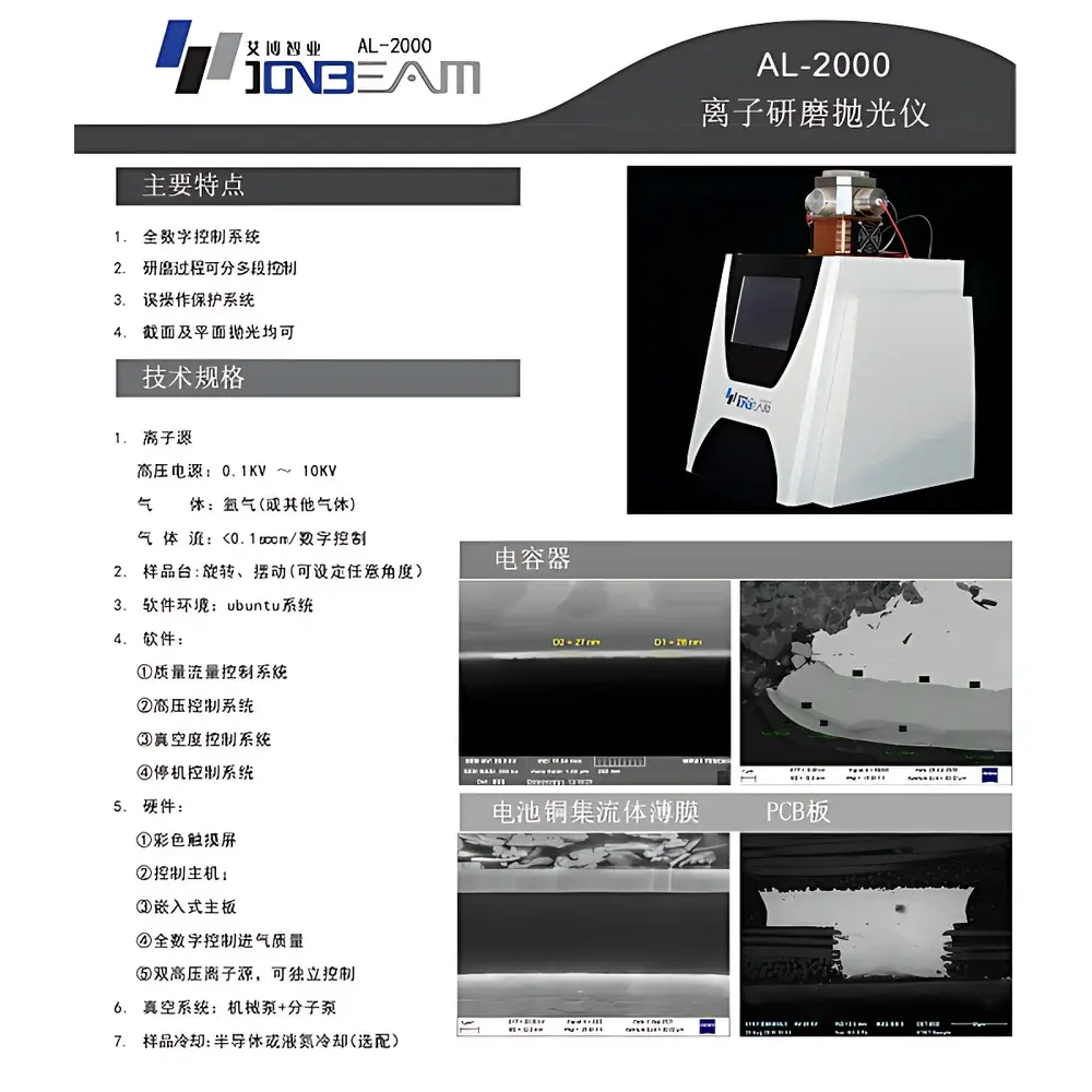
| Brand | Abbe / Ionbeam |
|---|---|
| Origin | Beijing, China |
| Manufacturer Type | OEM Manufacturer |
| Region Category | Domestic (China) |
| Model | AL-2000 |
| Pricing | Upon Request |
| Sample Diameter Capacity | Ø0–25 mm |
| Ultimate Vacuum | 5 × 10⁻³ Pa (without Ar gas) |
| Acceleration Voltage Range | 200–10,000 V |
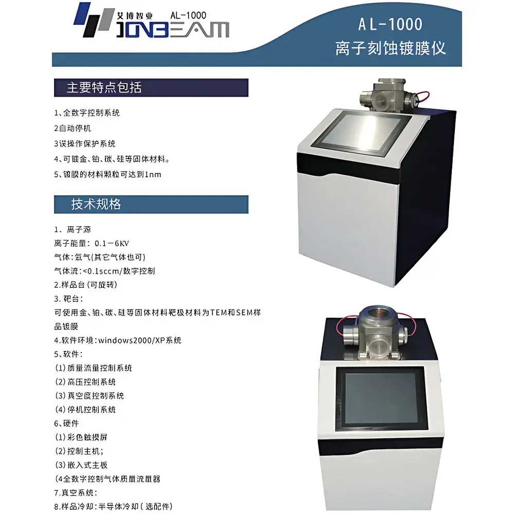
| Brand | Abel/Ionbeam |
|---|---|
| Origin | Beijing, China |
| Manufacturer Type | Direct Manufacturer |
| Region Classification | Domestic (China) |
| Model | AL-1000 |
| Pricing | Upon Request |
| Maximum Sample Diameter | Ø25 mm and Ø50 mm |
| Minimum Particle Size | ~3 nm |
| Ion Beam Energy Range | 200–6000 V |
| Base Vacuum | ≤5×10⁻³ Pa (without Ar flow) |
| Sample Stage | Motorized Rotation |
| Cooling Option | Peltier-based Semiconductor Cooling (optional) |
| Integrated Functions | Plasma Cleaning + Ion Beam Sputtering + Reactive Ion Beam Etching (with reactive gas inlet) |
| Control System | Digital Automated Controller with Real-time Parameter Logging |
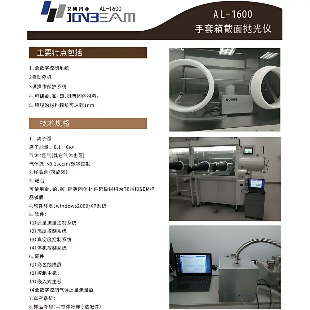
| Brand | Abel/Ionbeam |
|---|---|
| Origin | Beijing, China |
| Manufacturer | Yes |
| Country of Origin | China |
| Model | AL-1600 |
| Vacuum Base Pressure | ≤5×10⁻³ Pa (without Ar flow) |
| Acceleration Voltage Range | 200–6000 V |
| Sample Stage | Rotatable |
| Ion Source | Single Ion Gun |
| Cooling Option | Thermoelectric (optional) |
| Glovebox Integration | Yes |
| Primary Functions | Plasma Cleaning, Ion Beam Sputter Deposition, Reactive Ion Beam Etching (with reactive gas introduction) |
| Beam Uniformity | Optimized for Ø25 mm and Ø50 mm substrates |
| Typical Deposited Grain Size | ~3 nm |
| Low-Energy Ion Impact | Minimized substrate damage, suitable for thermally sensitive samples |
| In-situ Cleaning & Deposition | Integrated within single vacuum chamber |
| Control System | Digital, Programmable, Automated |
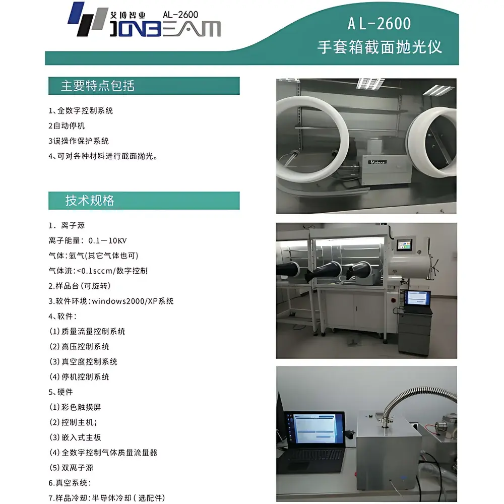
| Brand | Abel / Ionbeam |
|---|---|
| Origin | Beijing, China |
| Manufacturer Type | Direct Manufacturer |
| Product Category | Domestic |
| Model | AL-2600 |
| Pricing | Upon Request |
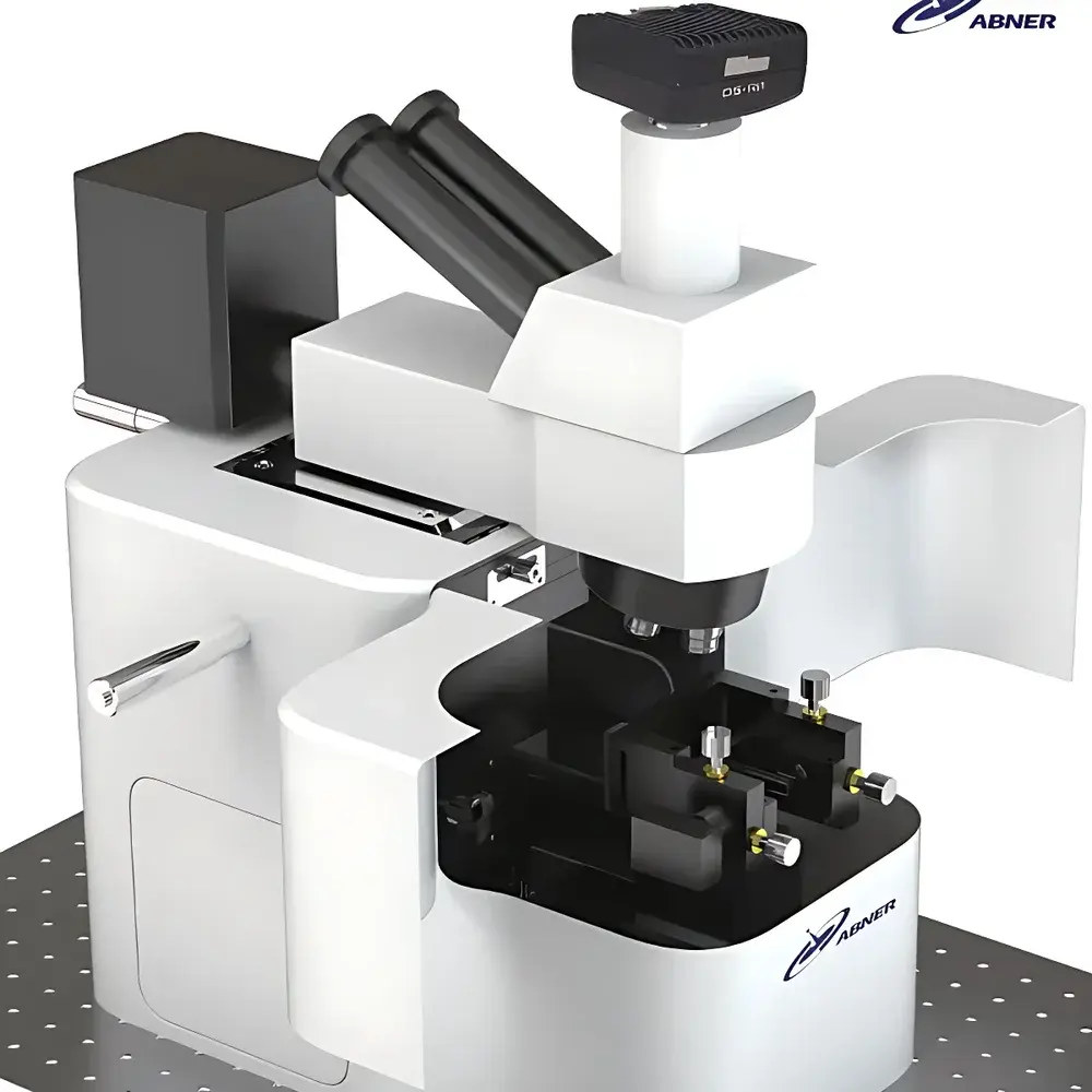
| Brand | Abner |
|---|---|
| Origin | Jiangsu, China |
| Model | ABN-AFM-001 |
| Instrument Type | Material-oriented AFM |
| Sample Dimensions | Max 15 mm × 15 mm × 2 mm |
| Scan Range | 70 µm × 70 µm (X–Y), 17 µm (Z) |
| Lateral Resolution | ≤1 nm |
| Vertical Resolution | ≤0.1 nm |
| XY Noise | ≤0.01 nm RMS |
| Z Noise | ≤0.05 nm RMS |
| Scan Speed | Up to 10 Hz |
| Probe Compatibility | Si probes with spring constants from 0.01 N/m to 40 N/m |
| Scanner | High-precision closed-loop piezoelectric scanner |
| Environmental Requirements | 18–25 °C, ≤60% RH |
| Image Resolution | 512×512 to 2048×2048 pixels |
| Interface | USB and Ethernet |
| Power Supply | 220 V/50 Hz or 110 V/60 Hz |
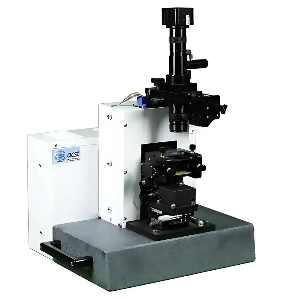
| Brand | ACST |
|---|---|
| Origin | USA |
| Manufacturer Type | Authorized Distributor |
| Origin Category | Imported |
| Model | ACST-AFM |
| Instrument Type | Biological AFM |
| Position Detection Noise | ≤0.15 nm RMS |
| Maximum Sample Size | 15 mm diameter |
| XY Stage Travel Range | 25 mm × 25 mm |
| Software | Aotu AFM |
| Imaging Modes | Contact, Tapping, Phase, Lateral Force, Advanced Force Spectroscopy, Conductive AFM, Magnetic AFM, Nanolithography |
| XY Scanner Range | >50 µm (closed-loop), <10 nm resolution (closed-loop), <1 nm resolution (open-loop) |
| Z Scanner Range | >16 µm |
| Z Sensor Noise | <5 nm |
| Z Feedback Noise | <0.2 nm |
| Z Actuation | Direct-drive stepper motor, 25 mm travel, 330 nm minimum step, 8 mm/min max speed |
| Optical System | 3 MP CCD camera, 45×–400× real-time magnification |
| Base Material | Solid granite for vibration isolation and mechanical stability |
| Probe Loading | Tool-free, rapid exchange design |
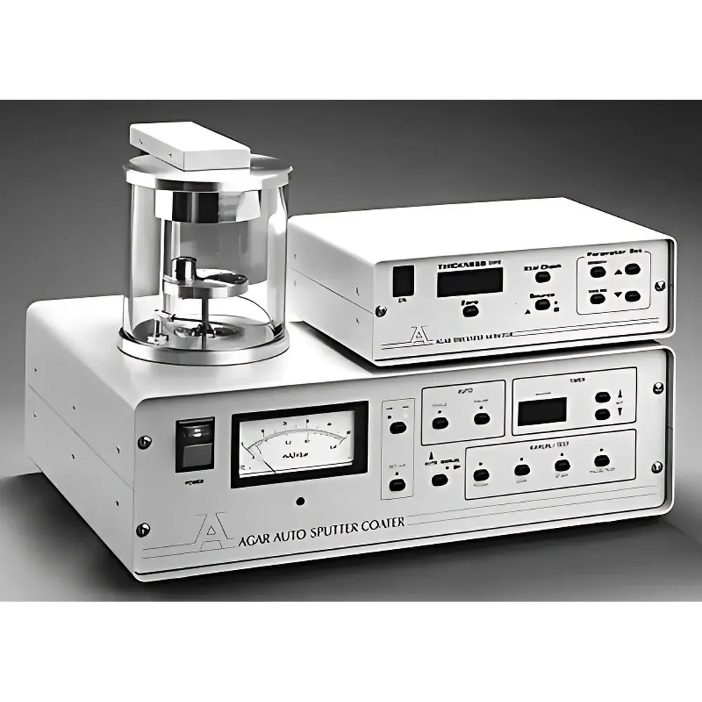
| Brand | Agar Scientific / Oxford Instruments |
|---|---|
| Origin | UK |
| Model | AGB7341 |
| Chamber Dimensions | 120 mm Ø × 120 mm H (optional 150 mm × 165 mm) |
| Sample Stage Capacity | 12 standard pin-type stubs |
| Stage Height Adjustment Range | 0–60 mm |
| Sputter Head | Low-voltage planar magnetron |
| Target Diameter/Thickness | 57 mm Ø × 0.1 mm |
| Standard Target Material | Au |
| Optional Targets | Pt, Au/Pd, Pt/Pd, Ag |
| Max Current | 40 mA |
| Current Control Range | 0–50 mA |
| Vacuum Range | Atmosphere to 1 × 10⁻³ mbar |
| Process Gas | Argon (≥99.9% purity) |
| Pumping Speed | 2 L/s mechanical pump |
| Power Supply | 220 V, 50/60 Hz |
| Digital Timer | 0–300 s with pause function |
| Safety Features | Vacuum interlock, over-current protection |
| Optional Quartz Crystal Thickness Monitor | In-situ nanoscale monitoring (resolution: 0.1 nm) |
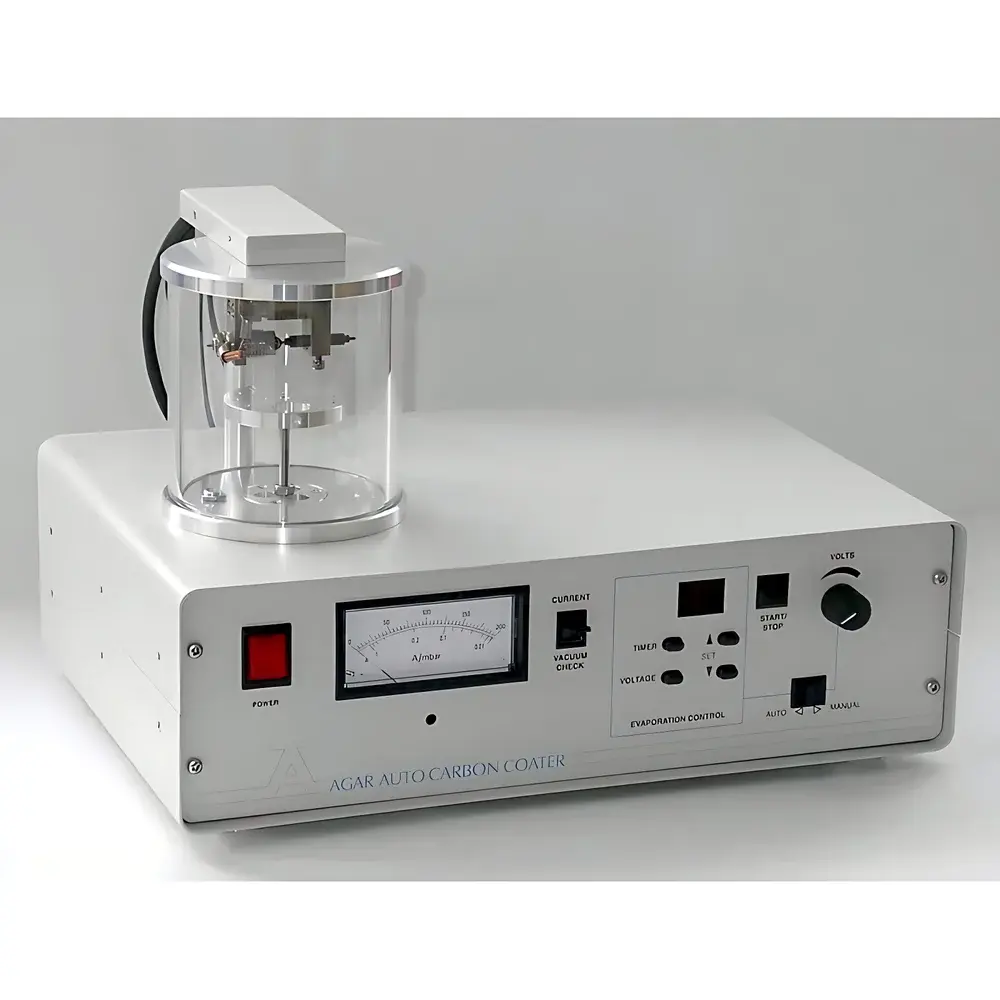
| Brand | Agar Scientific / Oxford Instruments |
|---|---|
| Origin | United Kingdom |
| Model | AGB7367A |
| Chamber Dimensions | 120 mm Ø × 120 mm H (glass) |
| Sample Stage | Stainless steel, accommodates up to 12 pin-type stubs, height adjustable over 30 mm range |
| Evaporation Source | High-purity graphite rod, 6.15 mm diameter |
| Power Control | Microprocessor-based, remote voltage/current sensing |
| Max Current | 180 A |
| Voltage Range | 0.1–5.5 V (digital setpoint) |
| Current Range | 0–200 A |
| Vacuum Gauge | Analog, 1 atm to 0.001 mbar |
| Pumping Speed | 2 L/s mechanical pump, reaches ≤0.1 mbar in 25–30 s |
| Operating Voltage | 220 V, 50/60 Hz |
| Optional QCM Thickness Monitor | 6 MHz quartz crystal, in-situ nanometric resolution (±0.1 nm for carbon) |
| Safety | Vacuum interlock, overcurrent protection |
| Operation Modes | Automatic (programmable timer: 1–30 s) and manual |
| Auto-vent Function | Yes |
| Compatibility | Zeiss, JEOL, Hitachi, Thermo Fisher (FEI), Tescan, Phenom SEM platforms |
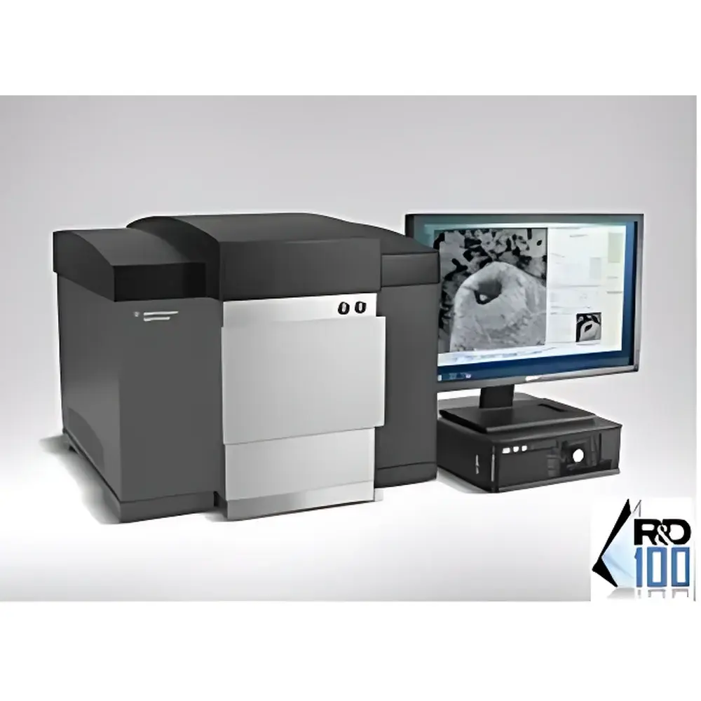
| Origin | USA |
|---|---|
| Manufacturer Type | Authorized Distributor |
| Origin Category | Imported |
| Model | 8500 |
| Price Range | USD 135,000 – 205,000 (FOB) |
| Electron Gun Type | Cold Field-Emission (CFE) |
| Secondary Electron Imaging Resolution | 10 nm @ 1 kV |
| Magnification Range | 250× – 800,000× |
| Accelerating Voltage | 0.5 – 2.0 kV |
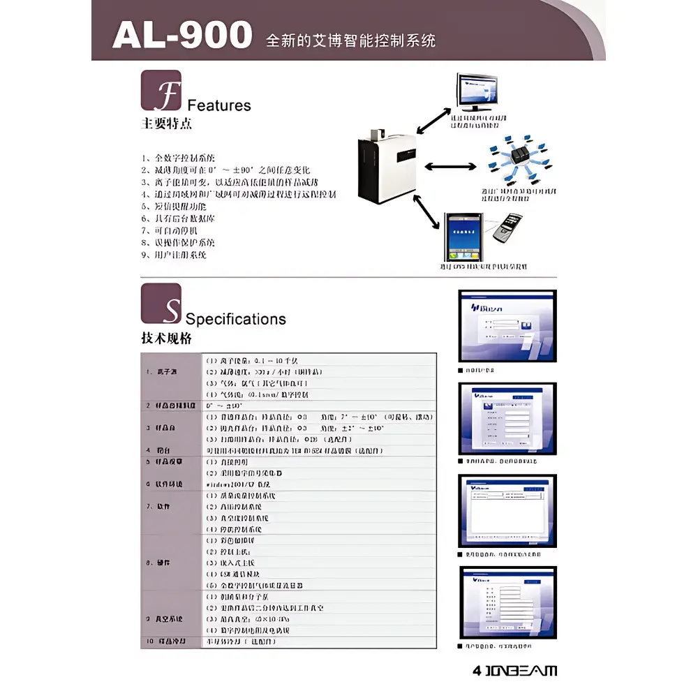
| Brand | Aibo |
|---|---|
| Origin | Beijing, China |
| Manufacturer Type | Direct Manufacturer |
| Country of Origin | China |
| Model | AL-900 |
| Pricing | Available Upon Request |
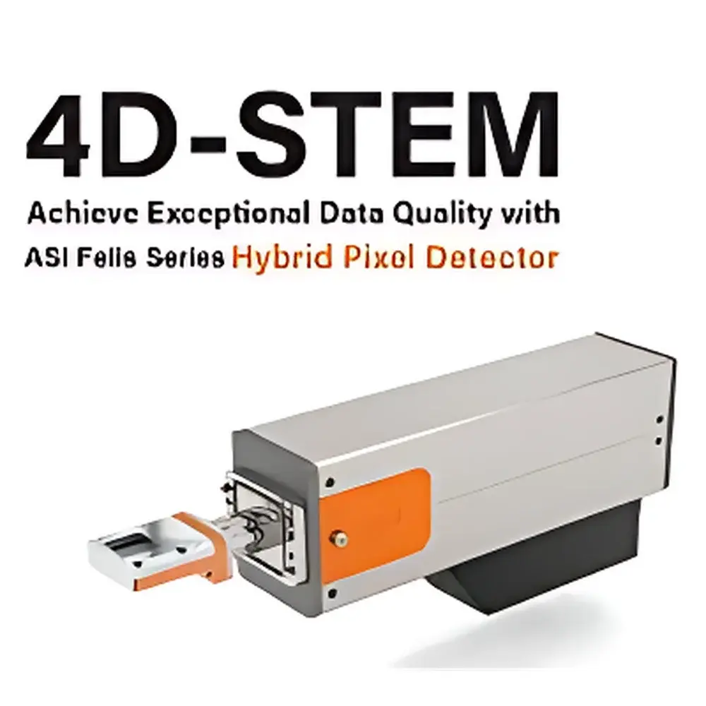
| Brand | Amsterdam Scientific Instruments (ASI) |
|---|---|
| Origin | Netherlands |
| Model | Felis T3 |
| Acceleration Voltage Range | 0.5–30 kV |
| Sample Stage | 5-position 3 mm TEM grid holder |
| Detector Type | Hybrid pixel detector with nanosecond timestamping capability |
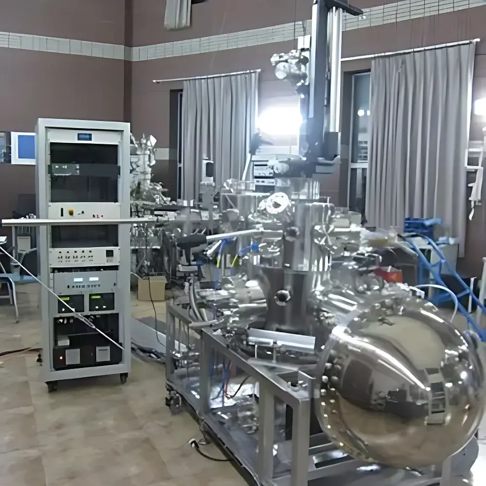
| Brand | Angstrom |
|---|---|
| Origin | USA |
| Model | ELS5000 |
| Energy Resolution | 0.7 meV |
| Angular Resolution | 0.08° (momentum resolution ≈ 0.002 Å⁻¹ at 7.4 eV incident energy) |
| Optical Architecture | 4-grid tungsten electron optics, UHV-compatible, no polymer-coated or fiberglass-insulated wiring |
| Field of View | 103° |
| Electron Gun Diameter | 1.59 cm |
| Retractable Optics | Standard 2-inch to optional 4-inch retraction |
| Compatibility | AES-compatible, ARPES-integrated capable |
| Detection Modes | pA–nA current range with integrated lock-in amplifier and MCP detector |
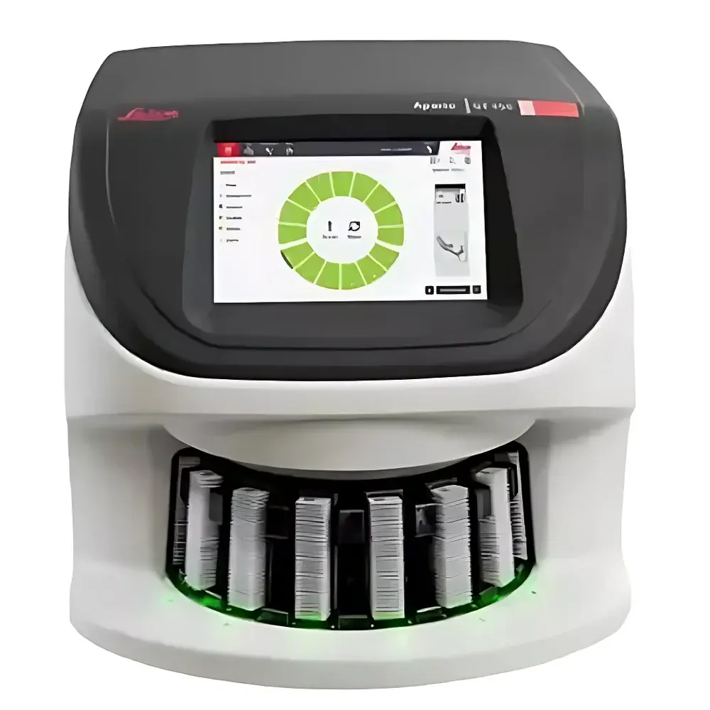
| Brand | Leica |
|---|---|
| Origin | Germany |
| Manufacturer Type | Authorized Distributor |
| Import Status | Imported |
| Model | Aperio GT450 |
| Electron Source | Cerium Hexaboride (CeB₆) |
| Scan Speed | 32 s per 15 mm × 15 mm area at 40× |
| Throughput | 81 slides/hour |
| Color Calibration | ICC-compliant medical-grade color profile (DICOM GSDF & sRGB aligned) |
| Optical System | Custom Leica 40× apochromatic objective with real-time autofocus |
| Intended Use | For Research Use Only (RUO) |
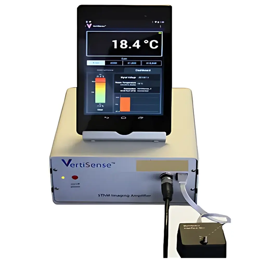
| Brand | AppNano |
|---|---|
| Origin | USA |
| Manufacturer Type | Authorized Distributor |
| Product Category | Imported Instrument |
| Model | VertiSense |
| Instrument Type | Material Science AFM-Compatible SThM Module |
| Primary Function | Nanoscale Thermal Property Mapping (Topography + Thermal Conductivity + Temperature Distribution) |
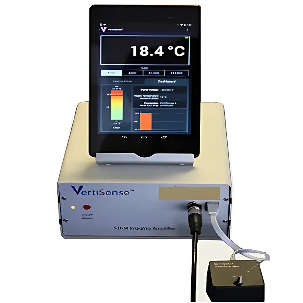
| Origin | USA |
|---|---|
| Manufacturer Type | Distributor |
| Origin Category | Imported |
| Model | VertiSense |
| Price Range | USD 14,000 – 72,000 (based on AFM integration configuration) |
| Instrument Type | Atomic Force Microscope (AFM)-Compatible Thermal Scanning Probe Module |
| Temperature Resolution | ≤ 10 mK (dependent on host AFM electronics and thermal calibration) |
| Spatial Thermal Resolution | ≤ 20 nm (tip-limited, under optimal vacuum/low-noise conditions) |
| Maximum Tip Operating Temperature | 700 °C |
| Sample Stage Compatibility | Fully compatible with standard commercial AFM sample stages (e.g., Bruker Dimension, Keysight 5500, Park Systems XE-series, Nanosurf Flex-Axiom) |
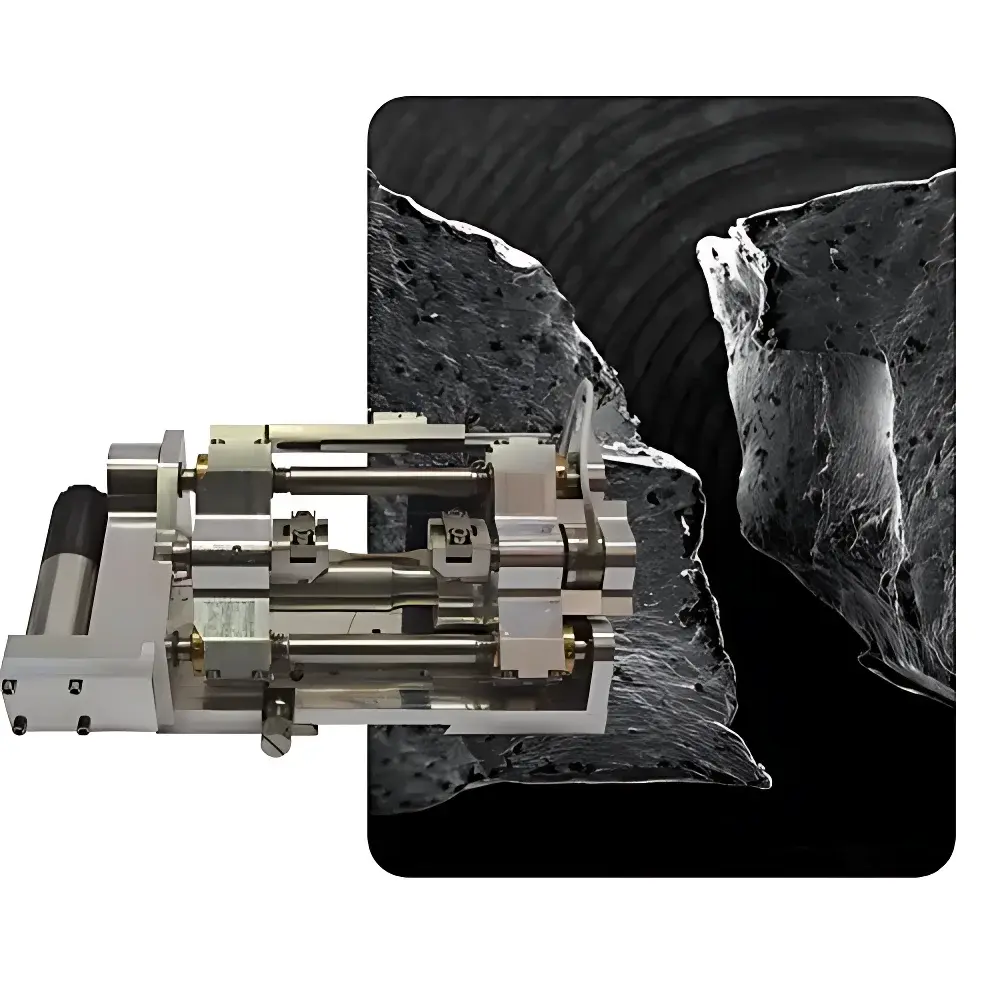
| Brand | Appo |
|---|---|
| Origin | United Kingdom |
| Model | SWIFT |
| Max Load Capacity | 10 kN |
| Temperature Range | –120 °C to +1000 °C |
| Stroke Range | 16–26 mm |
| Compatibility | SEM, TEM, Optical Microscope, Confocal Microscope, EBSD, Raman, XRD, AFM, Metallographic Microscope |
| Control Interface | Windows 10–compatible PC-based controller with drag-and-drop test sequencing software |
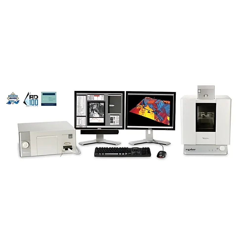
| Brand | Oxford Instruments |
|---|---|
| Origin | Germany |
| Manufacturer Type | Authorized Distributor |
| Origin Category | Imported |
| Model | GetReal |
| Price Range | USD 13,500 – 68,000 |
| Instrument Type | AFM Calibration Module |
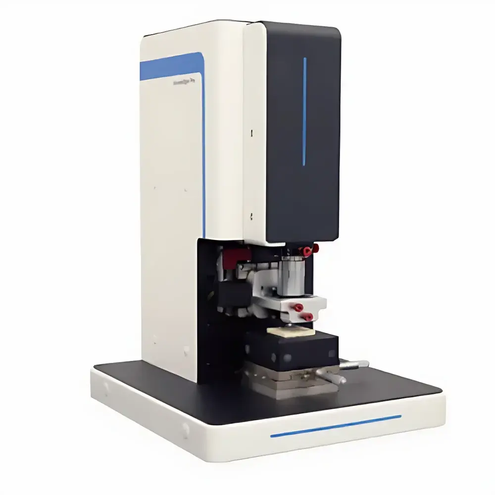
| Brand | Truth Instruments Company Limited |
|---|---|
| Origin | Beijing, China |
| Manufacturer Type | Authorized Distributor |
| Country of Origin | China |
| Model | AtomEdge Pro |
| Pricing | Available Upon Request |
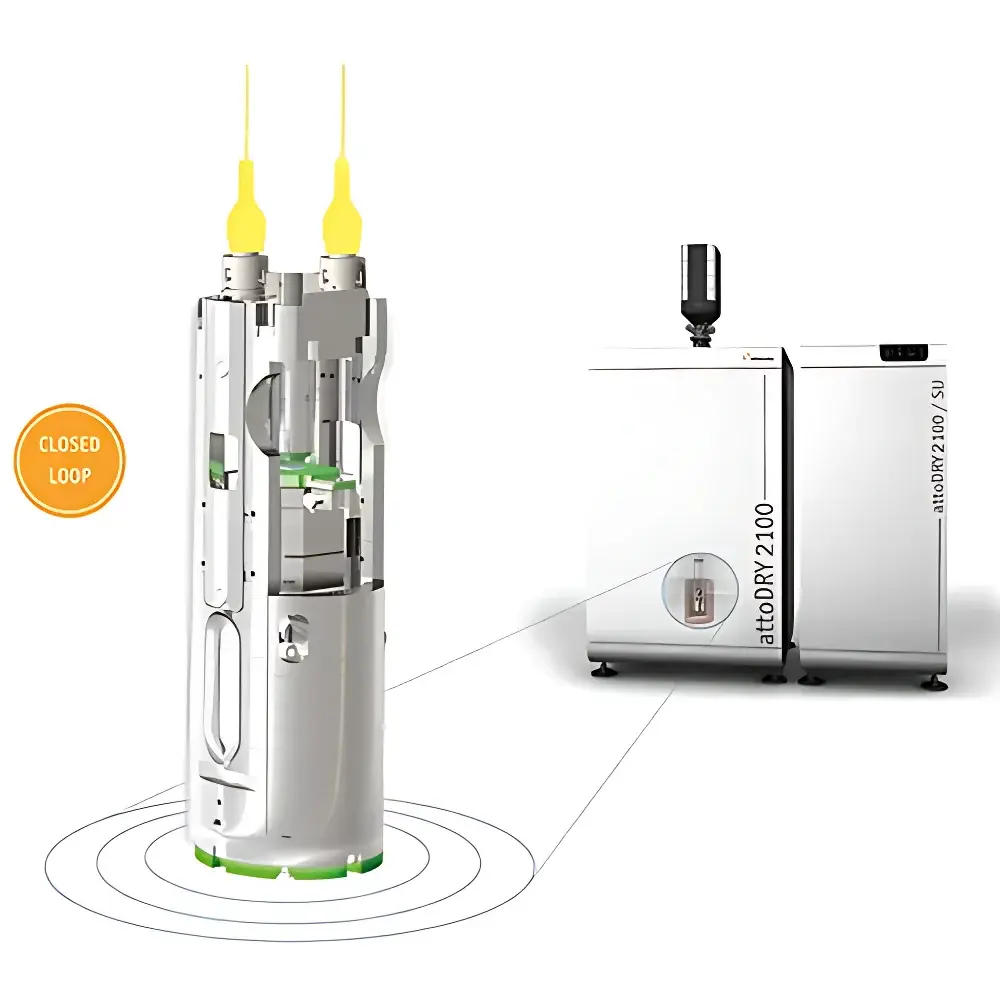
| Brand | attocube |
|---|---|
| Origin | Germany |
| Model | attoCFM I |
| Instrument Type | Cryogenic Confocal Microscope for Quantum Materials Research |
| Positioning Noise | < 0.5 nm |
| Sample Size Capacity | Ø100 mm |
| Sample Stage Travel Range | 150 µm (fine scan) / 5 × 5 × 5 mm³ (coarse positioning) |
| Temperature Range | 1.8 K – 300 K |
| Magnetic Field | Up to 12 T (vector magnet optional) |
| Vacuum Operating Range | 1 × 10⁻⁶ mbar – 1 atm |
| Optical Resolution | ~550 nm (at 635 nm, NA = 0.82) |
| Scan Area | 30 × 30 µm² @ 4 K |
| Objective | Cryo-optimized Achromatic Objective, NA = 0.82, WD = 0.7 mm |
| Expandable Modules | AFM/MFM/PFM/KPFM/ct-AFM/cryo-Raman |
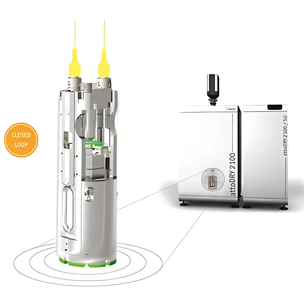
| Brand | attocube |
|---|---|
| Origin | Germany |
| Model | attoCFM I |
| Instrument Type | Magnetic Force Microscope (MFM) / Cryogenic Confocal Microscope |
| Positioning Noise | < 0.5 nm |
| Sample Size Capacity | Ø100 mm |
| Sample Stage Travel Range | 150 µm (fine scan) / 5 × 5 × 5 mm³ (coarse positioning) |
| Temperature Range | 1.8 K – 300 K |
| Magnetic Field | Up to 12 T (vector magnet optional) |
| Vacuum Operation | 1 × 10⁻⁶ mbar – 1 atm |
| Numerical Aperture (NA) | 0.82 |
| Optical Resolution | ~550 nm (@635 nm) |
| Working Distance (WD) | 0.7 mm |
| Confocal Scan Range | 30 × 30 µm² @4 K |
| Compatible Cryostats | attoDRY1000/2100, Quantum Design PPMS (1″/2″ bore) |
| Expandable Modules | AFM/MFM/PFM/KPFM/ct-AFM/cryo-Raman |
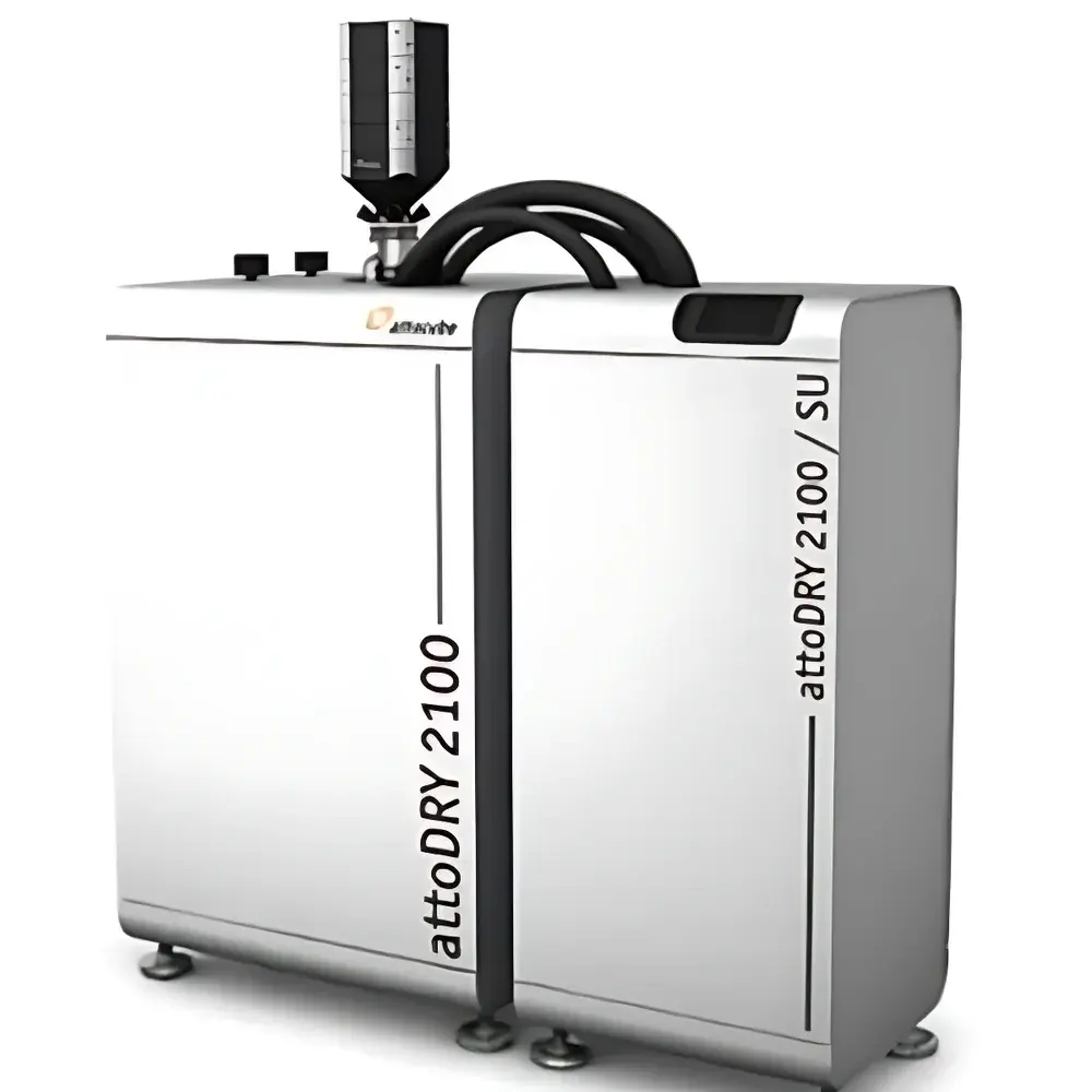
| Brand | Attocube Systems AG |
|---|---|
| Origin | Germany (manufactured in Germany |
| Instrument Type | Research-grade industrial SPM platform |
| Magnet Strength | Up to 15 T |
| Temperature Range | 1.5 K – 300 K (continuous, closed-cycle) |
| Positioning Noise | < 0.5 nm RMS |
| Sample Dimensions | Max 100 mm × 50 mm × 20 mm |
| XY Scanner Range | 10 µm × 10 µm |
| Vibration Level | 0.12 nm RMS (typical) |
| Compliance | ASTM E2579, ISO/IEC 17025 compatible operation environment |
| Software Control | Integrated touchscreen interface with automated temperature/magnetic field ramping |
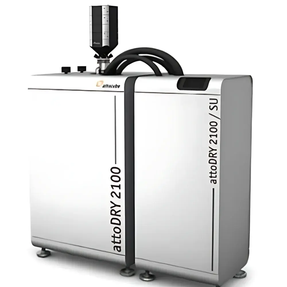
| Brand | Attocube Systems AG |
|---|---|
| Origin | Germany |
| Model | attoDRY Lab |
| Instrument Type | Cryogenic Scanning Probe Microscope (SPM) |
| Magnetic Field Strength | Up to 15 T |
| Temperature Range | 1.5 K – 300 K (closed-cycle) |
| Positioning Noise | < 0.5 nm RMS |
| Sample Dimensions | Max 100 mm × 50 mm × 20 mm |
| XY Scanner Range | 10 µm × 10 µm |
| Vibration Level | 0.12 nm RMS (typ.) |
| Compliance | ASTM E2917, ISO/IEC 17025 compatible workflows, GLP/GMP-ready data logging |
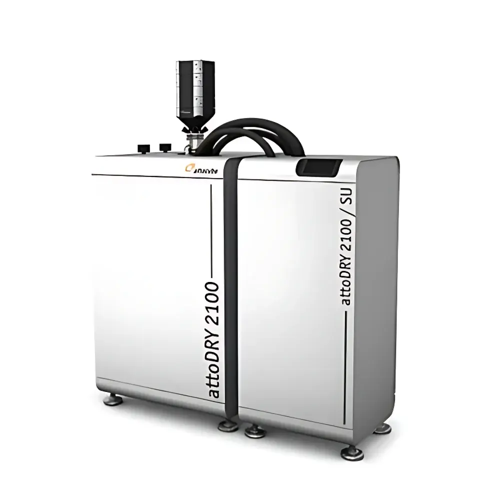
| Brand | Attocube Systems AG |
|---|---|
| Origin | Germany |
| Model | attoDRY Lab |
| Instrument Type | Magnetic Force Microscope (MFM) |
| Positioning Noise | 0.12 nm RMS |
| Sample Stage Travel Range | 5 mm × 5 mm × 5 mm |
| Temperature Range | 1.5 K – 300 K (configurable) |
| Maximum Magnetic Field | 15 T |
| Cooling Time (to base temperature) | ~1–2 hours |
| Control Interface | Integrated touchscreen with automated thermal and magnetic field sequencing |
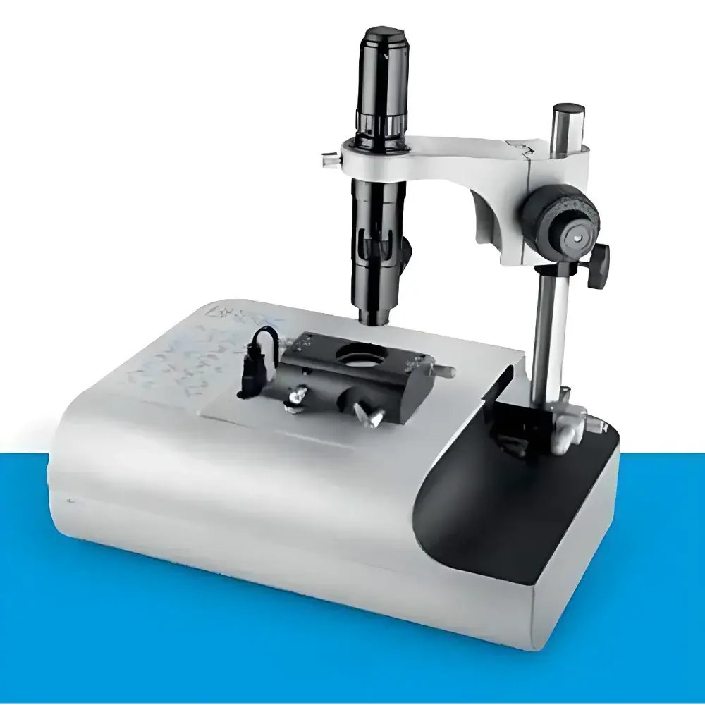
| Brand | Auniontech |
|---|---|
| Origin | Shanghai, China |
| Manufacturer Type | Authorized Distributor |
| Product Origin | Domestic (China) |
| Model | AFM-Portable Series |
| Pricing | Available Upon Request |
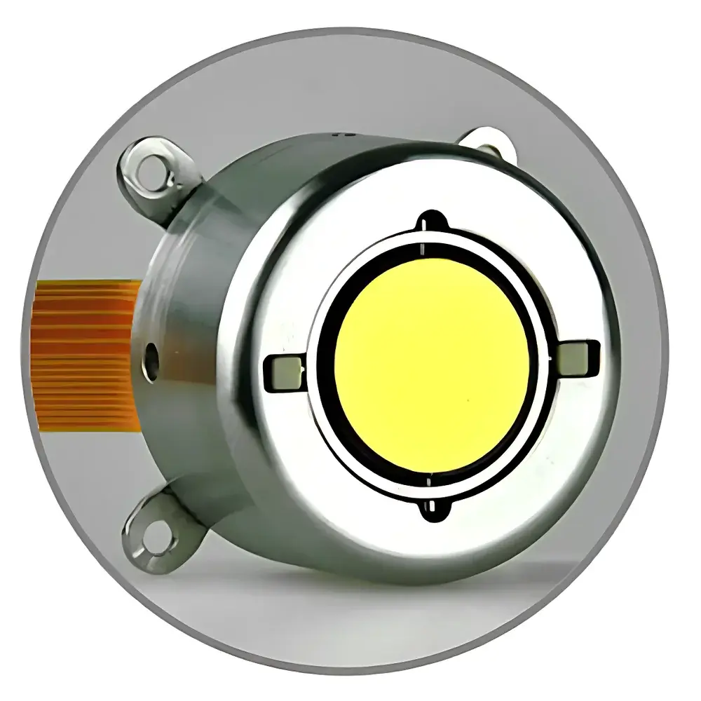
| Brand | Auniontech |
|---|---|
| Model | W |
| Actuator Type | 4-Quadrant (2-axis, bi-directional) |
| Mechanical Tilt Angle (DC) | ±25° (X & Y axes) |
| Mirror Diameter | 15 mm |
| Center of Rotation to Mirror Surface | 1.3 mm |
| External Diameter | 30 mm |
| Zero Drift | ≤25 µrad/°C |
| Closed-Loop Resolution | <5 µrad |
| Repeatability (RMS, typical) | 30–100 µrad |
| Full-Scale Bandwidth (Sine, ±25°) | 20 Hz |
| Small-Signal Bandwidth | 350 Hz |
| Large-Angle Step Response (20° step) | 7.5 ms |
| Small-Angle Step Response (0.1° step) | 1.4 ms |
| Instrument Form Factor | Benchtop |
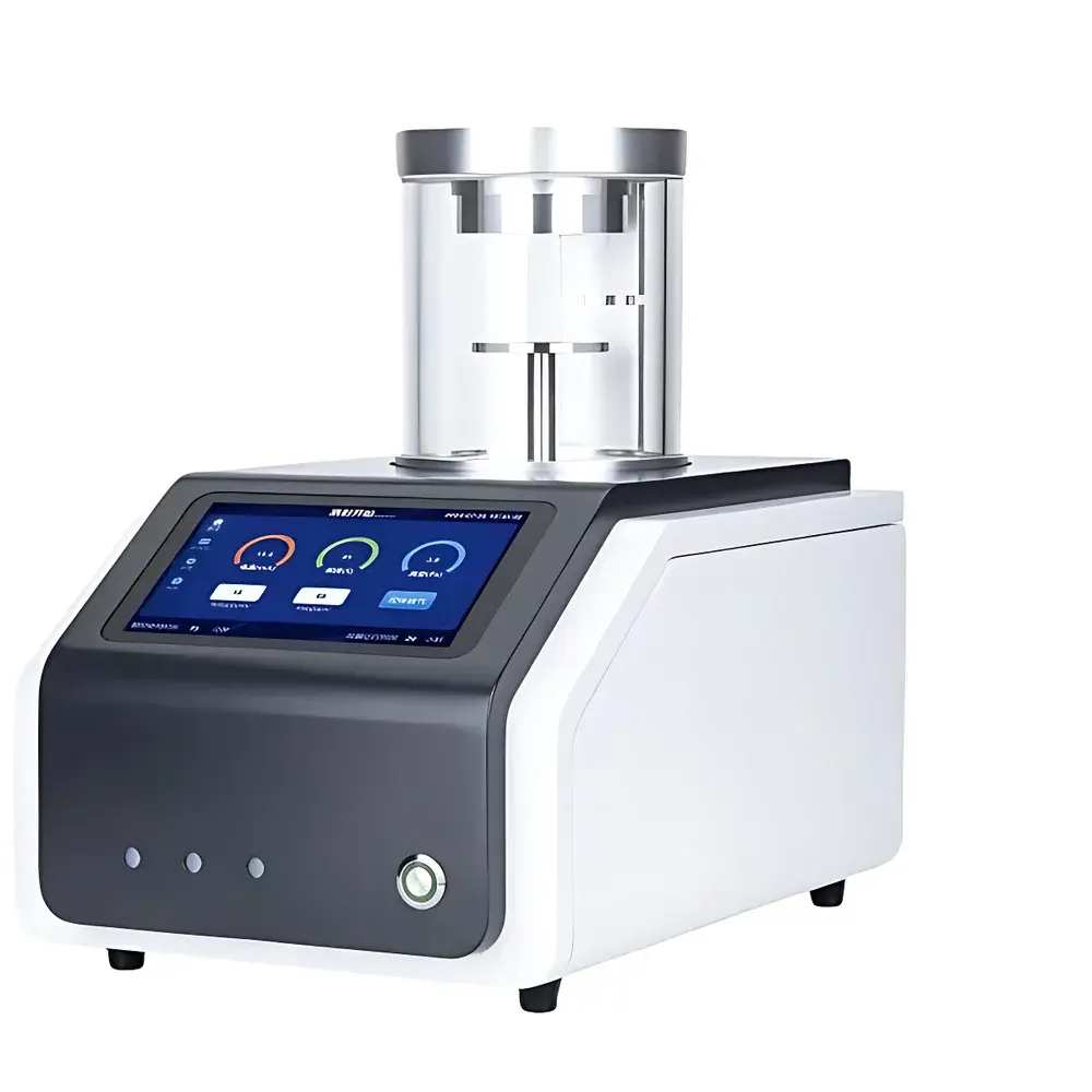
| Brand | Beam Convergence |
|---|---|
| Model | GVC2000 |
| Origin | Beijing, China |
| Manufacturer Type | Direct Manufacturer |
| Country of Origin | China |
| Pricing | Upon Request |
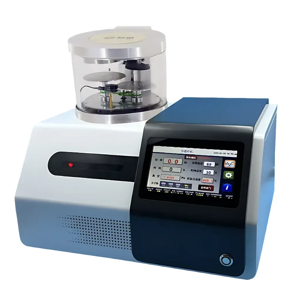
| Brand | Beam Convergence |
|---|---|
| Origin | Beijing, China |
| Manufacturer Type | Direct Manufacturer |
| Model | GVC5000T |
| Dimensions | 480(L)×390(D)×460(H) mm |
| Power Supply | 220 VAC / 1200 W |
| Sputtering Target Diameter | φ57 mm |
| Sputtering Current Range | 5–200 mA |
| Sputtering Time Range | 0–999 s |
| Evaporation Source | φ0.8 mm Carbon Fiber |
| Evaporation Sources | 1–4 units |
| Evaporation Modes | Continuous & Pulsed |
| Vacuum Chamber | Borosilicate Glass, φ200×130 mm |
| Base Pressure | <5×10⁻³ Pa |
| Pumping Speed | 90 L/s (Turbo) + 1.1 L/s (Rotary) |
| Pump-Down Time | ≤5 min to 5×10⁻³ Pa |
| Human-Machine Interface | 7-inch TFT Color Touchscreen |
| Maximum Sample Stage Diameter | φ125 mm |
| Pre-Sputtering | Integrated Automatic Baffle |
| Protection Features | Overcurrent, Vacuum Interlock, Turbo Pump Thermal Protection |
| Anti-Contamination Design | Dual-Isolation Architecture for Sputtering & Evaporation Modules |
| Optional Quartz Crystal Thickness Monitor | Real-time Thickness Display, Setpoint Control, Resolution: 0.1 nm, Range: 1–999 nm per cycle, Max. Measurable Thickness: 10 μm |
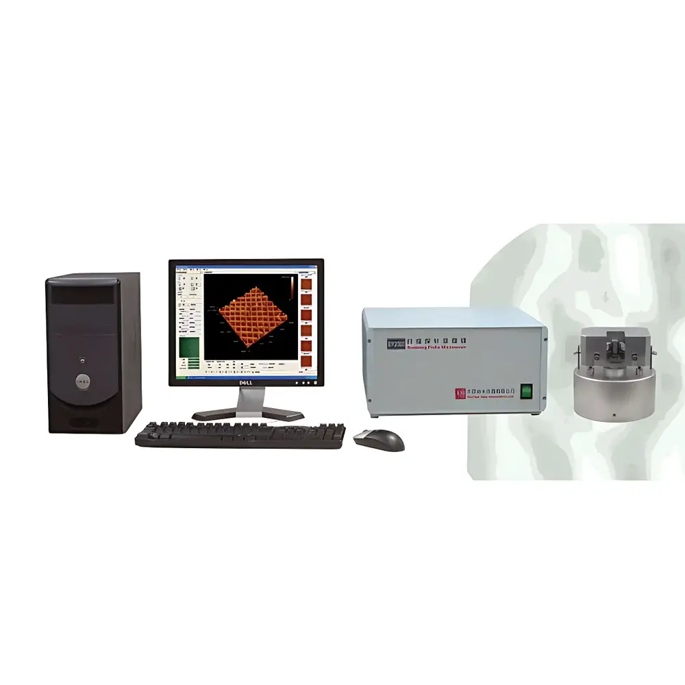
| Brand | Benyuan Nano |
|---|---|
| Origin | Beijing, China |
| Manufacturer Type | Authorized Distributor |
| Product Origin | Domestic (China) |
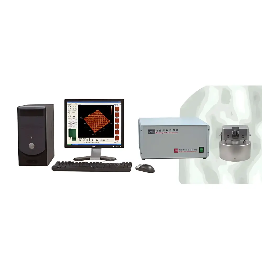
| Model | BY1000 |
| Price Range | USD 14,000 – 70,000 |
| Instrument Type | Scanning Tunneling Microscope (STM) |
| Position Detection Noise | 0.1 Å RMS |
| Maximum Sample Size | Ø45 mm × 15 mm |
| XY Sample Stage Travel Range | 100 mm × 100 mm |
| Brand | Benyuan Nano |
|---|---|
| Origin | Beijing, China |
| Manufacturer Type | Authorized Distributor |
| Country of Origin | China |
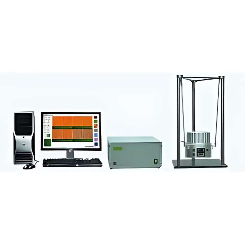
| Model | BY3000 |
| Price Range | USD 14,000 – 72,000 |
| Instrument Type | Atomic Force Microscope (AFM) |
| Position Detection Noise | 0.1 nm |
| Maximum Sample Diameter | 45 mm |
| Maximum Sample Thickness | 15 mm |
| XY Sample Stage Travel Range | 100 mm × 100 mm |
| Brand | BENYUAN Nano |
|---|---|
| Model | CSPM5500 |
| Origin | Beijing, China |
| Instrument Type | Atomic Force Microscope (AFM) with integrated Scanning Tunneling Microscope (STM) and Lateral Force Microscope (LFM) |
| Position Detection Noise | 0.1 nm |
| Sample Diameter Limit | <102 mm (4 in) |
| Sample Thickness Limit | <40 mm |
| XY Sample Stage Travel Range | 100 mm × 100 mm |
| Maximum Z-Travel (Auto-Approach) | >30 mm |
| Image Resolution | Up to 4096 × 4096 physical pixels |
| Horizontal Resolution (AFM) | 0.2 nm (mica-calibrated) |
| Vertical Resolution (AFM) | 0.1 nm (mica-calibrated) |
| Horizontal Resolution (STM) | 0.1 nm (graphite-calibrated) |
| Vertical Resolution (STM) | 0.01 nm (graphite-calibrated) |
| Data Interface | Fast Ethernet (10/100 Mbps) or USB 2.0 |
| Real-Time 3D Visualization | Yes |
| PID-Controlled Force Feedback | Yes |