
Electron Microscope
Filter
Showing 61–90 of 532 results

| Brand | Bruker |
|---|---|
| Origin | Germany |
| Model | ESPRIT QUBE |
| Compatibility | Integrated with Bruker e-Flash EBSD detectors and QUANTAX EDS systems |
| Data Format Support | HDF5, .ctf, .ang, .h5ebsd, .edax, .oxford, .bmp, .tiff |
| Licensing | Concurrent or node-locked perpetual license |
| System Requirements | Windows 10/11 (64-bit), ≥32 GB RAM, ≥2 TB SSD storage recommended, NVIDIA GPU with ≥8 GB VRAM (CUDA 11.2+) |
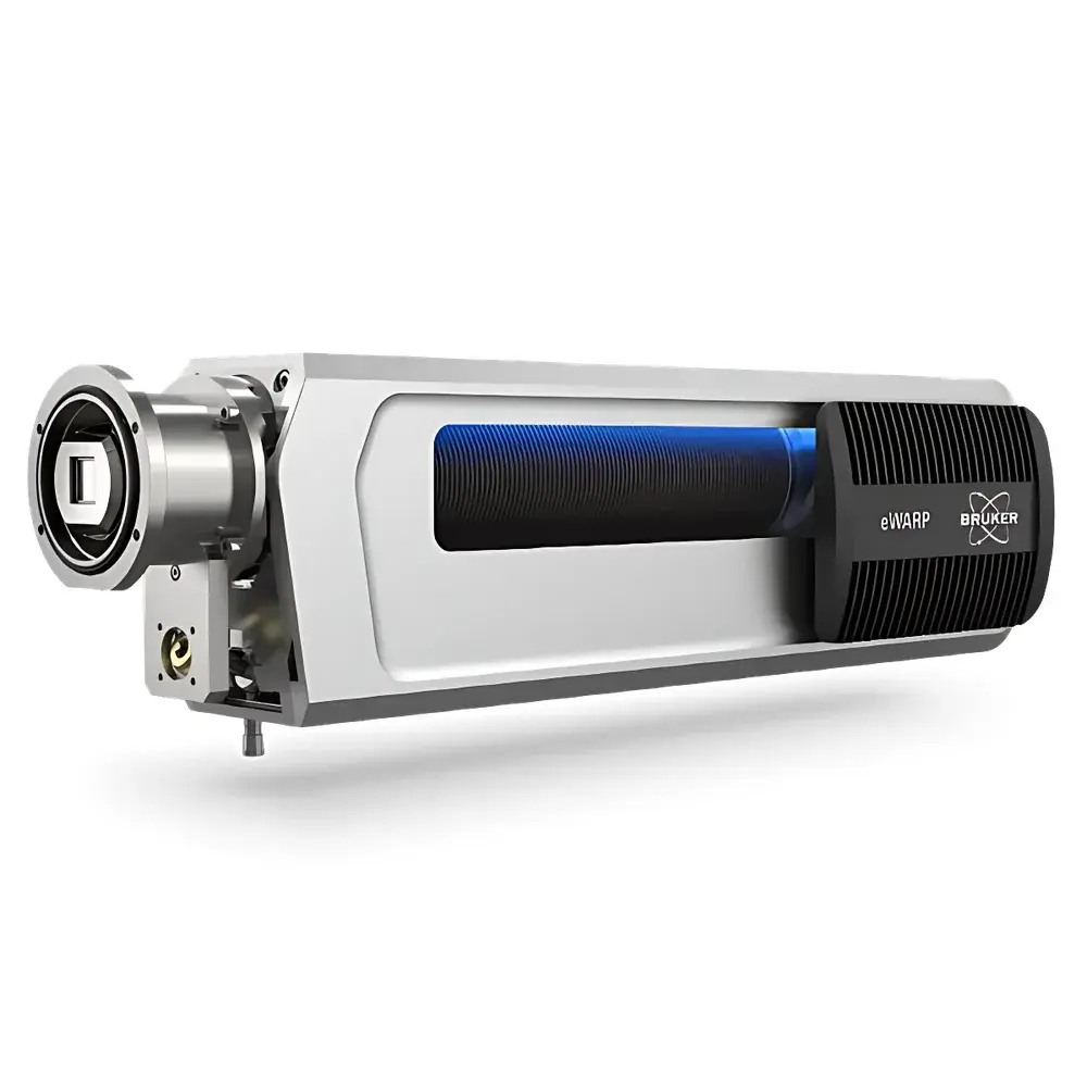
| Brand | Bruker |
|---|---|
| Origin | Germany |
| Manufacturer Type | Authorized Distributor |
| Origin Category | Imported |
| Model | eWARP |
| Quotation | Upon Request |
| Maximum Pattern Acquisition Rate | 14,400 patterns/second |
| Spatial Resolution | 20 nm |
| Angular Resolution | 0.1° |
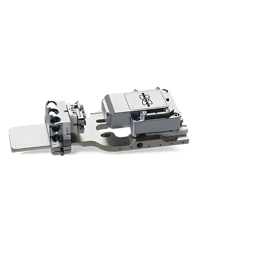
| Brand | Bruker |
|---|---|
| Origin | USA |
| Model | Hysitron PI 89 |
| Application | In-situ nanomechanical testing inside SEM and FIB/SEM chambers |
| Sensing Principle | Capacitive displacement sensing with sub-nanometer resolution |
| Actuation | Electromechanical force actuation |
| Force Range | Up to 100 mN (standard configuration) |
| Displacement Resolution | < 0.2 nm |
| Positioning Accuracy | ≤ 50 nm (with integrated linear encoder and motorized tilt/rotate stages) |
| Compatibility | Fully compatible with FEI/Thermo Fisher, Zeiss, JEOL, and Hitachi SEM/FIB platforms |
| Analytical Integration | Synchronized acquisition with EBSD, EDS, BSE, and TKD detectors |
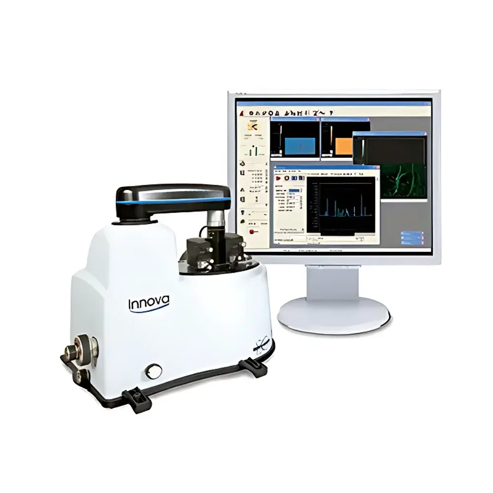
| Brand | Bruker |
|---|---|
| Origin | USA |
| Model | Innova |
| Instrument Type | Atomic Force Microscope (AFM) |
| Sample Stage Travel Range | 90 µm |
| Positional Detection Noise | < 0.1 nm (RMS, Z-axis, typical in air) |
| Maximum Sample Size Compatibility | 90 mm diameter × 25 mm height |
| Closed-Loop Scan Linearity | ±0.05% over full range |
| Z-Range | 10 µm (standard), upgradable to 15 µm |
| Optical Navigation Resolution | 1.3 MP color CCD with 4×–40× motorized zoom |
| AFM Mode Support | Contact, Tapping, Phase Imaging, Force Modulation, Lateral Force, Conductive AFM, Kelvin Probe Force Microscopy (KPFM), Magnetic Force Microscopy (MFM) |
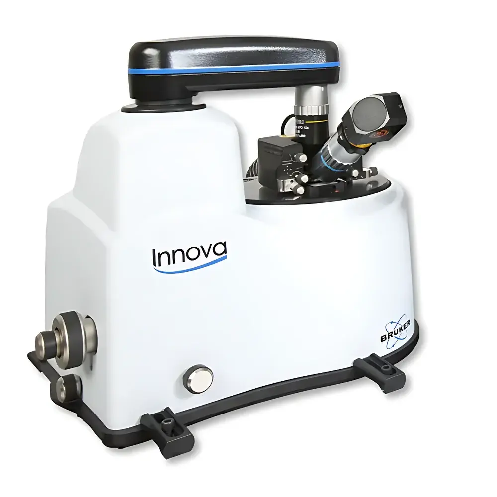
| Brand | Bruker |
|---|---|
| Origin | USA |
| Model | Innova |
| Instrument Type | Atomic Force Microscope (AFM) |
| Positioning Detection Noise | <2 µm (with standard 10× objective) |
| Sample Dimensions | 50 mm × 50 mm × 18 mm (X × Y × Z) |
| Z-Axis Stage Travel | 18 mm |
| Closed-Loop Scanner Range | XY > 90 µm, Z > 7.5 µm |
| Open-Loop Scanner Range | XY > 5 µm, Z > 1.5 µm |
| Optical Field of View | 1.24 mm × 0.25 mm (motorized zoom, 10× objective) |
| Optical Resolution | <2 µm (10×), <0.75 µm (50×) |
| Controller | 20-bit DAC, 100 kHz ±10 V ADCs |
| Software | SPMLab™ v7.0 (Windows® XP) |
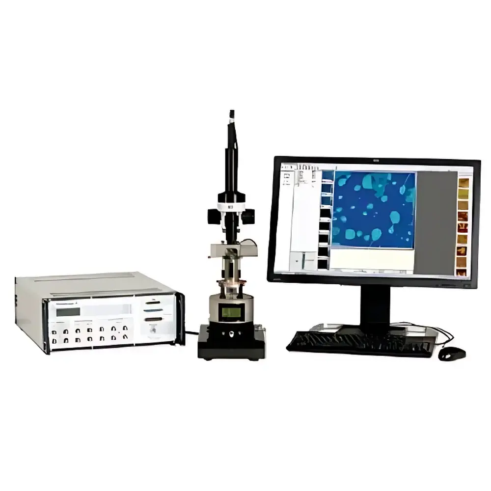
| Brand | Bruker |
|---|---|
| Origin | USA |
| Model | MultiMode 8 |
| Instrument Type | Atomic Force Microscope (AFM) |
| Z-Direction Positioning Noise | <0.3 Å RMS (Tapping Mode, 0 nm scan size, with active vibration isolation) |
| Maximum Sample Size | 15 mm × 15 mm × 5 mm |
| XY Stage Travel Range | 15 mm × 15 mm |
| Optional Scan Heads | AS-0.5 (0.4 µm × 0.4 µm XY / 0.4 µm Z), AS-12 (10 µm × 10 µm XY / 2.5 µm Z), AS-130 (125 µm × 125 µm XY / 5.0 µm Z), PF50 (40 µm × 40 µm XY / 20 µm Z) |
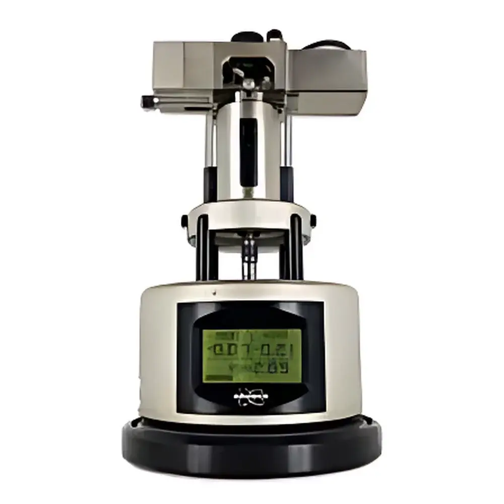
| Brand | Bruker |
|---|---|
| Origin | Germany |
| Model | MultiMode 8 |
| Instrument Type | Materials-Focused AFM |
| XY Positioning Noise | ≤0.15 nm |
| Maximum Sample Diameter | ≤15 mm |
| Maximum Sample Thickness | ≤5 mm |
| Sample Stage Travel Range | 180 mm × 180 mm (visible area) |
| Controller | NanoScope® V |
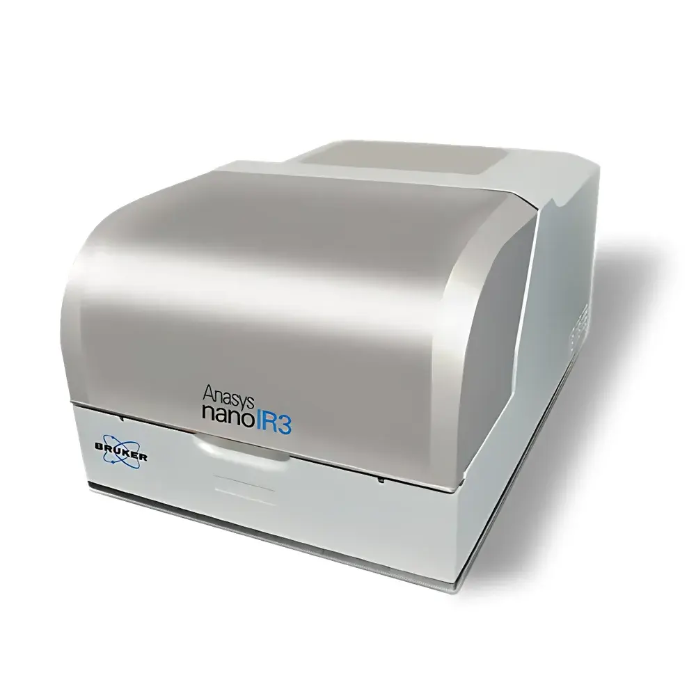
| Brand | Bruker |
|---|---|
| Origin | USA |
| Model | nanoIR3 |
| Instrument Type | Nano-Fourier Transform Infrared Spectrometer |
| Category | Scanning Probe Microscope–Integrated Optical Spectroscopy System |
| Compliance | ASTM E2947-21 (Standard Guide for Nanoscale Infrared Spectroscopy), ISO/IEC 17025–Accredited Measurement Capability Context |
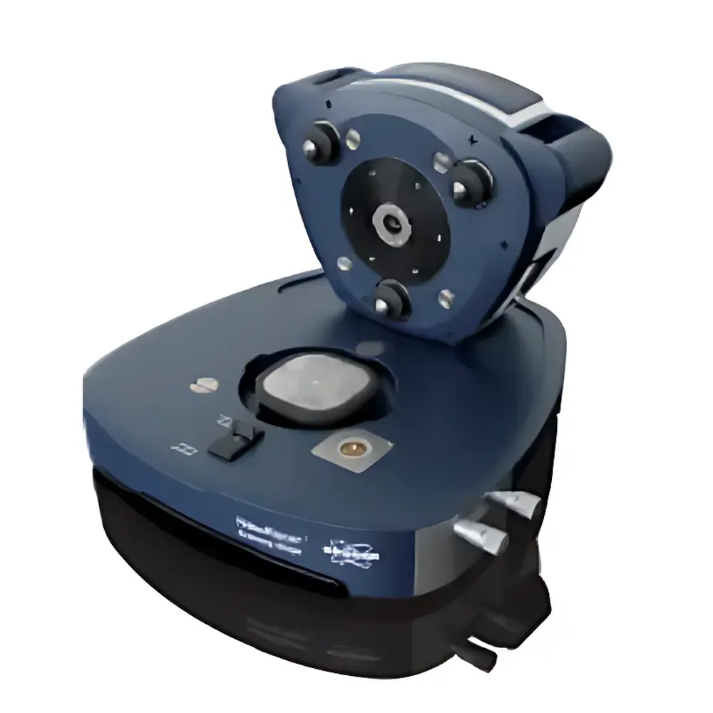
| Brand | Bruker |
|---|---|
| Origin | Germany |
| Manufacturer Type | Authorized Distributor |
| Origin Category | Imported |
| Model | NanoRacer |
| Instrument Type | Biological Atomic Force Microscope |
| XY Position Detection Noise | <0.09 nm RMS |
| Z Position Detection Noise | <0.04 nm RMS |
| Typical Sample Diameter | 4 mm |
| Software Version | V7 |
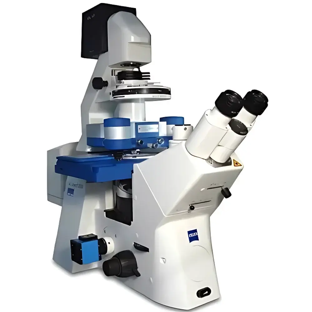
| Brand | Bruker |
|---|---|
| Origin | Germany |
| Model | NanoWizard 4 XP |
| Instrument Type | Biological Atomic Force Microscope |
| Position Detection Noise | X-Y direction RMS < 0.09 nm, Z direction RMS < 0.04 nm |
| Sample Scan Area | 100 µm × 100 µm × 15 µm |
| Stage Travel Range | 20 × 20 mm² |
| Software | V7 |
| Controller | Vortis™ 2 |
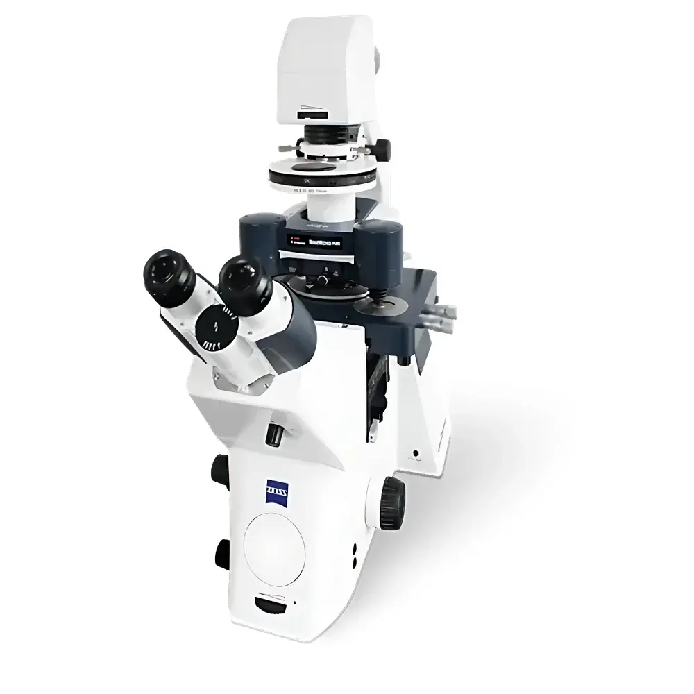
| Brand | Bruker |
|---|---|
| Origin | Germany |
| Model | NanoWizard PURE |
| Instrument Type | Biological Atomic Force Microscope |
| Category | Scanning Probe Microscope (SPM) |
| Architecture | Modular, Optically Compatible SPM Platform |
| Key Capabilities | Correlative Optical-AFM Imaging, Quantitative Nanomechanics, Multi-Modal Functional Imaging (PFM, MFM, EFM, KPFM, C-AFM, SSRM, STS, sThermal-AFM), Nanomanipulation & Nanolithography |
| Software Suite | JPK Instruments (now part of Bruker) SPMLab+, ExperimentalPlanner, RampDesigner, DirectOverlay2, DirectTiling |
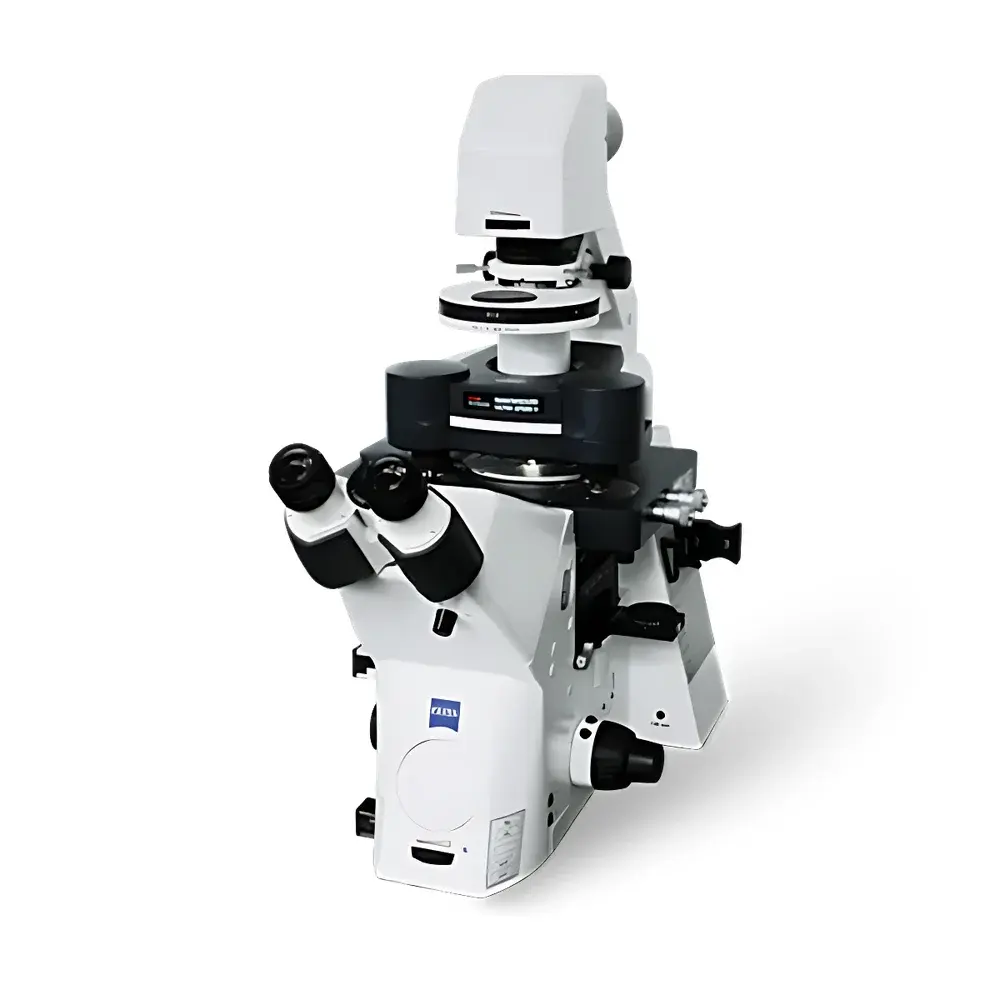
| Brand | Bruker |
|---|---|
| Origin | Germany |
| Model | ULTRA Speed 3 |
| Instrument Type | Biological Atomic Force Microscope |
| Category | Scanning Probe Microscope (SPM) |
| Architecture | Modular, Multi-Functional SPM Platform |
| Compliance | Designed for GLP/GMP-relevant environments with audit-trail-capable software |
| Data Format | Native HDF5 storage with metadata embedding |
| Automation Level | Fully integrated hardware-software automation for unattended operation |
| Software Framework | JPK Instruments’ BioAFM Suite (licensed and co-developed with Bruker) |
| Microscope Integration | Compatible with inverted optical microscopes (e.g., Zeiss Axio Observer, Nikon Ti2, Olympus IX83) |
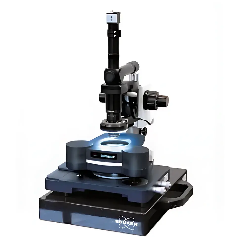
| Brand | Bruker |
|---|---|
| Origin | Germany |
| Model | NanoWizard V |
| Instrument Type | Biological Atomic Force Microscope |
| Sample Stage Travel Range | 20 × 20 mm² |
| Maximum Sample Height (with Head-Up Stage) | 140 mm Ø × 18 mm thickness |
| Free Sample Space | Ø140 × 18 mm³ |
| Software | V8 |
| Key Capabilities | PeakForce-QI, PeakForce Tapping®, PeakForce QNM®, Quantitative Imaging (QI), Single-Molecule Force Spectroscopy, Single-Cell Force Spectroscopy, DirectOverlay 2 for AFM–Optical Correlative Imaging, ExperimentPlanner & ExperimentControl modules, Integrated High-NA Optical Microscopy, Multi-Dimensional Environmental Control |
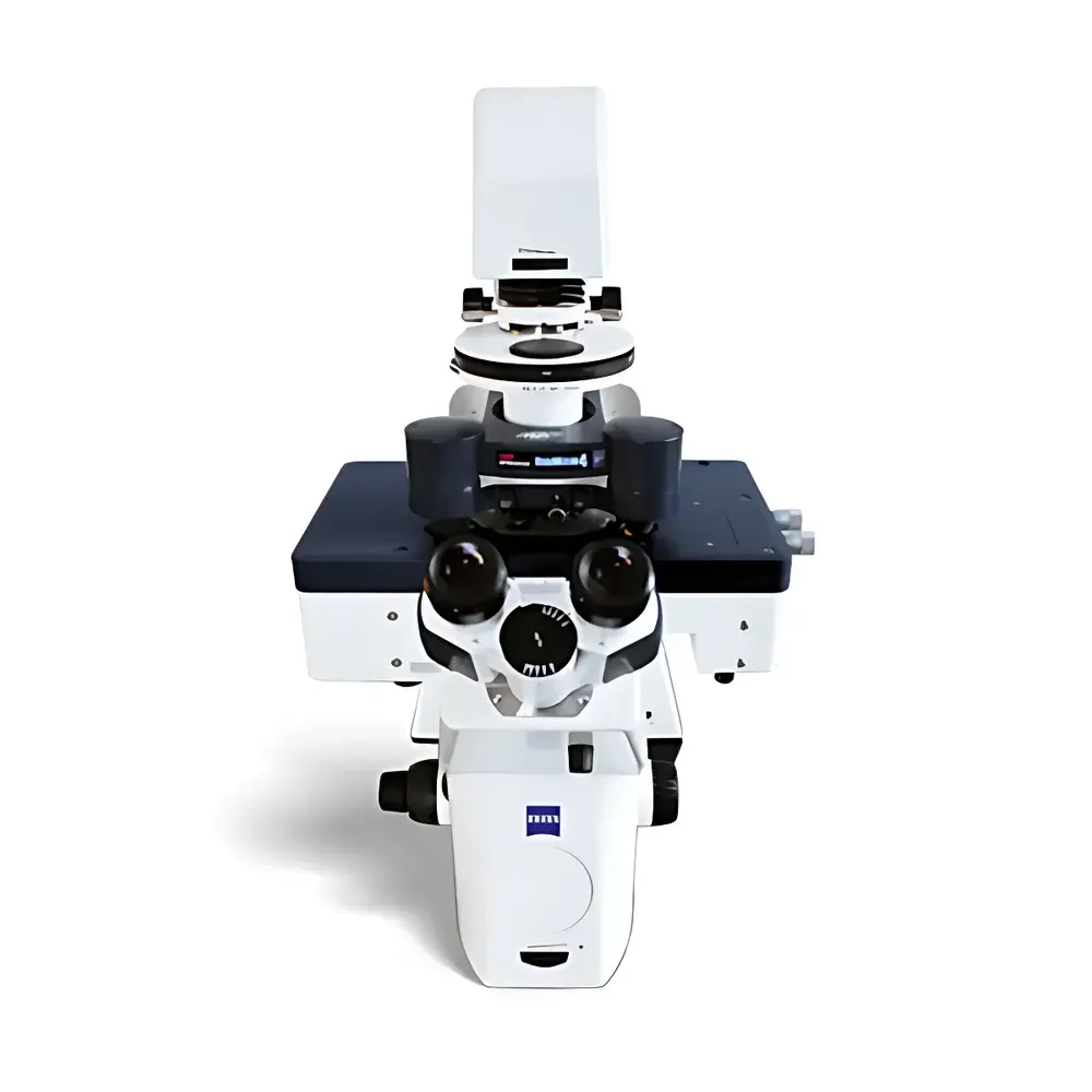
| Brand | Bruker |
|---|---|
| Origin | Germany |
| Model | NanoWizard® 4 XP BioScience |
| Instrument Type | Biological Atomic Force Microscope |
| Software Platform | V7 |
| Category | Scanning Probe Microscope |
| Import Status | Imported |
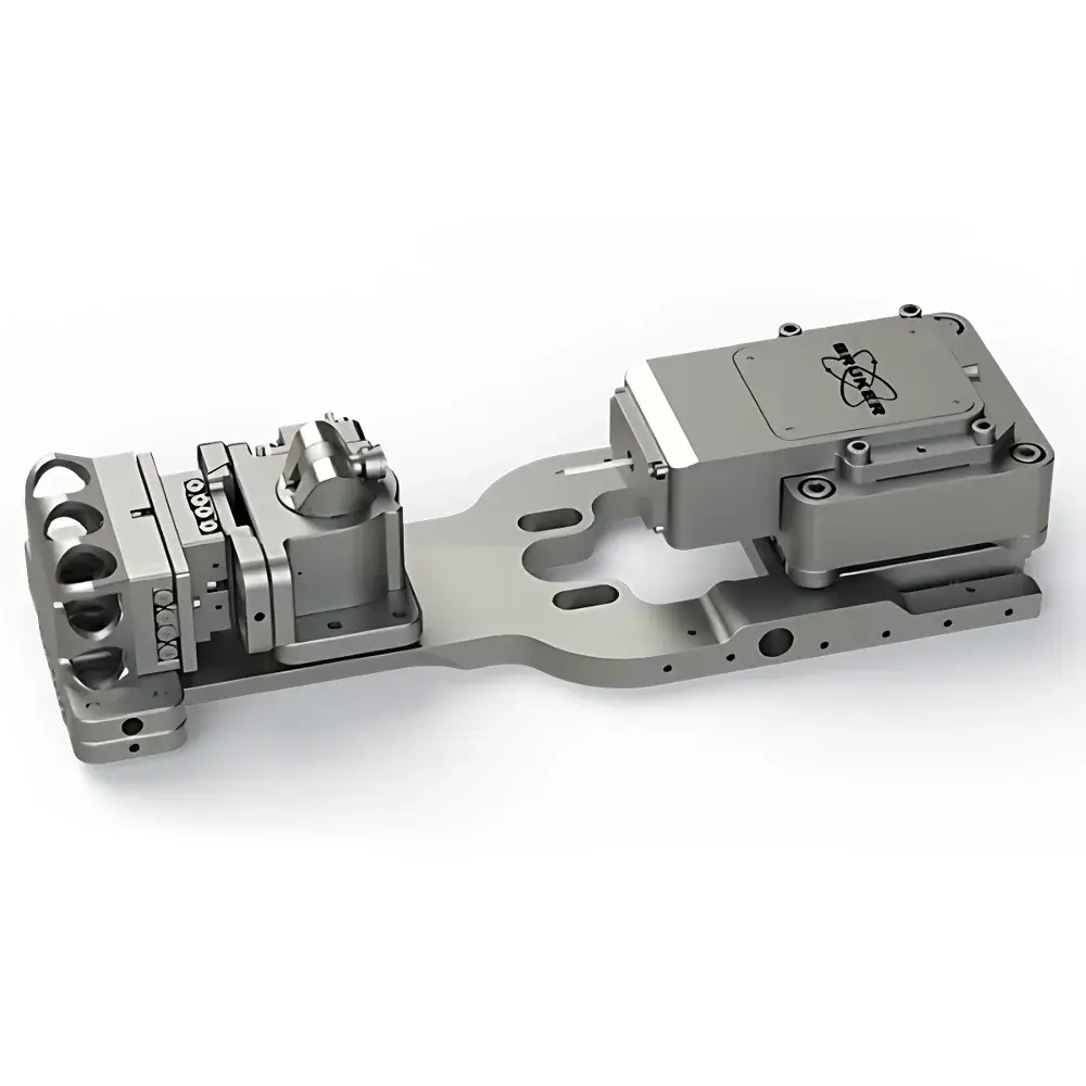
| Brand | Bruker |
|---|---|
| Origin | USA |
| Model | PI 89 AUTO |
| Application Domain | In situ SEM-integrated nanomechanical characterization |
| Automation Level | Fully motorized stage + patented dual-axis rotation/tilt (R/T) mechanism |
| Software Platform | TriboScan Auto v5.0+ |
| Compliance Framework | Designed for GLP-compliant workflows |
| Sample Environment | Compatible with standard high-vacuum and low-vacuum SEM chambers (FEI, Thermo Fisher, Zeiss, JEOL) |
| Maximum Load Resolution | Sub-100 nN |
| Displacement Resolution | < 0.05 nm |
| Stage Precision | ±50 nm positional repeatability over 10 mm × 10 mm travel range |
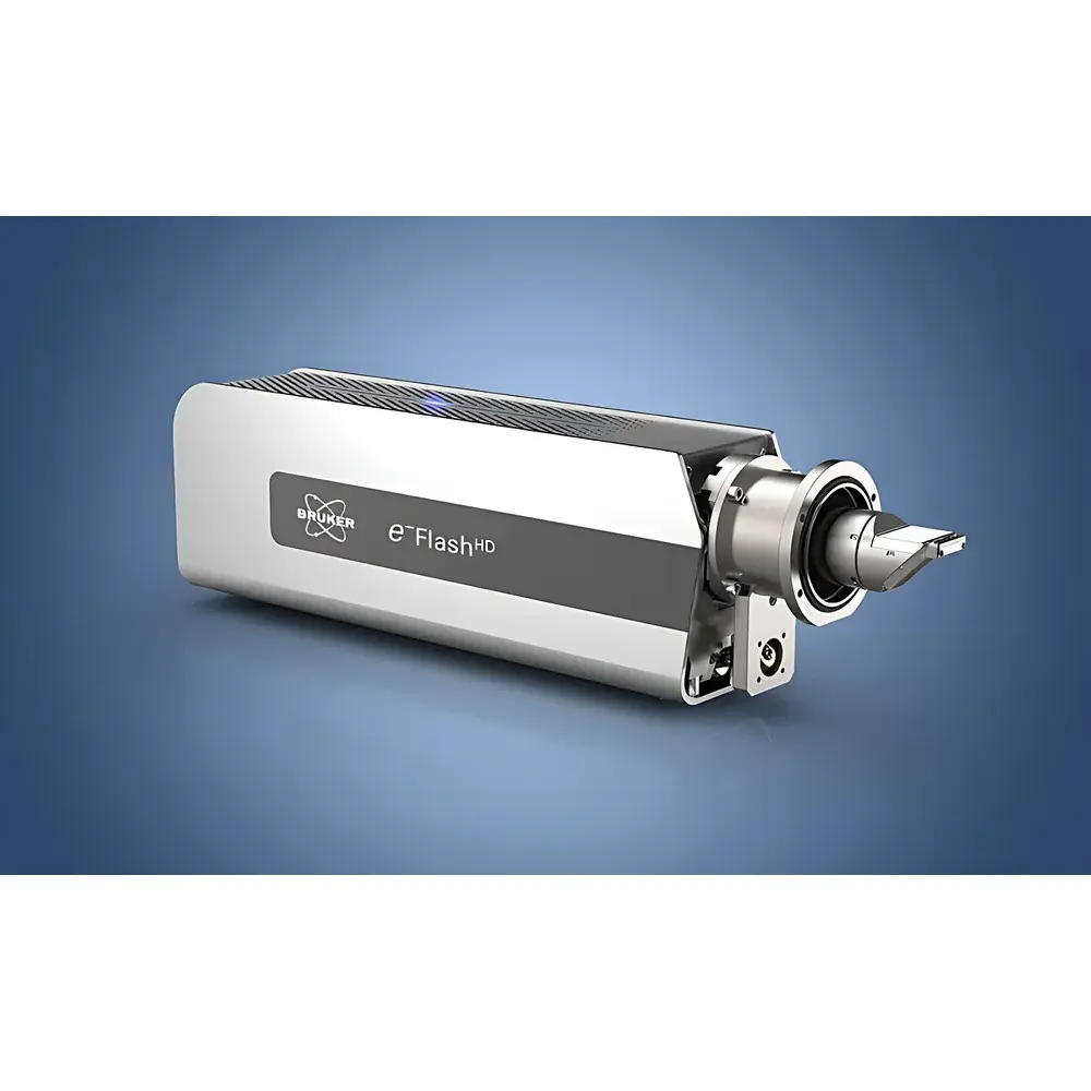
| Brand | Bruker |
|---|---|
| Origin | Germany |
| Manufacturer Type | Authorized Distributor |
| Origin Category | Imported |
| Model | QUANTAX EBSD |
| Pricing | Upon Request |
| CCD Camera Resolution | 640 × 480 pixels |
| Maximum Stage Speed | 10 mm/s |
| Spatial Resolution | 1.5 nm |
| Angular Resolution | 0.1° |
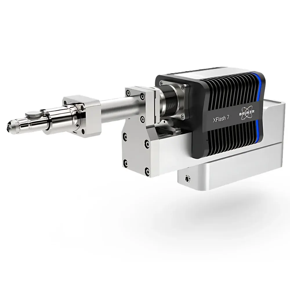
| Brand | Bruker |
|---|---|
| Origin | Germany |
| Manufacturer Type | Authorized Distributor |
| Origin Category | Imported |
| Model Series | QUANTAX Transmission Electron Microscopy (TEM/STEM) EDS |
| Energy Resolution | <129 eV |
| Peak-to-Background Ratio | 20,000:1 |
| Maximum Count Rate | 1500 kcps |
| Elemental Detection Range | Be to Cf |
| Detector Active Area | 10–300 mm² |
| Window Options | Polymer Ultrathin Window or Windowless |
| Brand | Bruker |
|---|---|
| Origin | Germany |
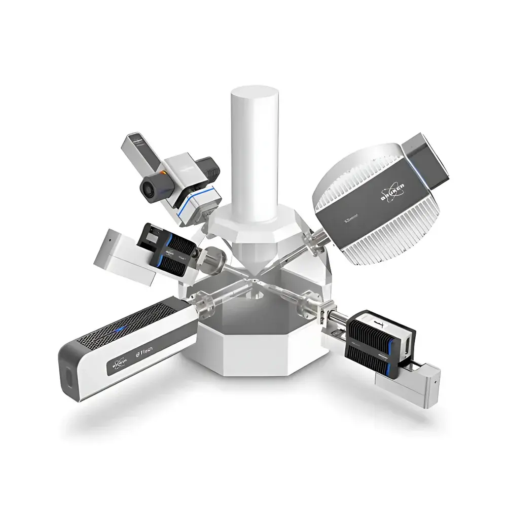
| Model | QUANTAX FlatQUAD |
| Energy Resolution | <129 eV |
| Peak-to-Background Ratio | 20,000:1 |
| Maximum Count Rate | 4,000 kcps |
| Elemental Detection Range | Boron (B) to Californium (Cf) |
| Detector Active Area | 10–300 mm² |
| Window Type | Windowless |
| Brand | Bruker |
|---|---|
| Origin | Germany |
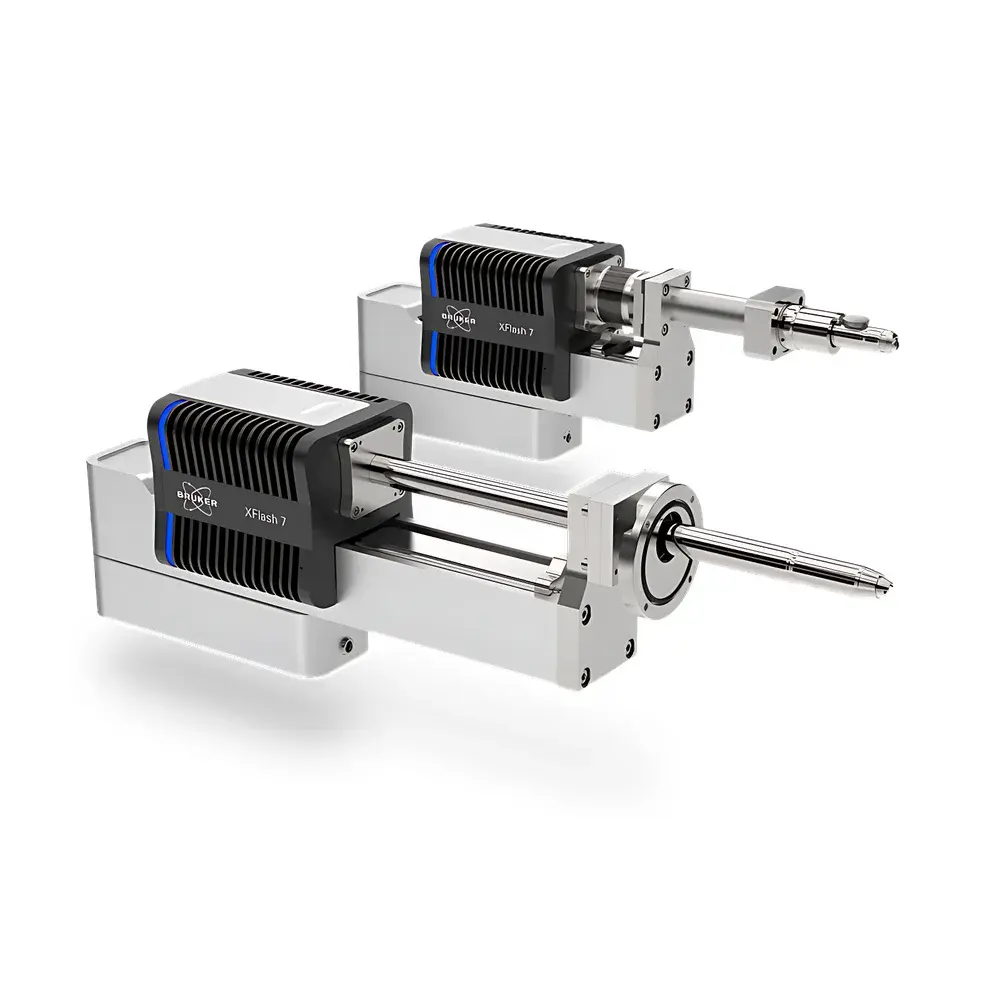
| Model | Quantax XFlash Series |
| Energy Resolution | <129 eV |
| Peak-to-Background Ratio | 20,000:1 |
| Maximum Count Rate | 1,500 kcps |
| Elemental Detection Range | Be to Cf |
| Detector Active Area | 10–300 mm² |
| Window Options | Ultrathin Polymer Window or Windowless Configuration |
| Brand | Bruker |
|---|---|
| Origin | Germany |
| Manufacturer Type | Authorized Distributor |
| Origin Category | Imported |
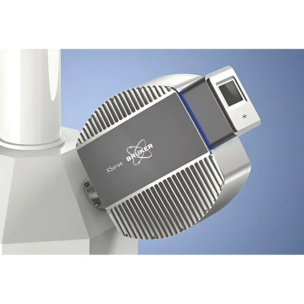
| Model | QUANTAX xsense |
| Pricing | Upon Request |
| Brand | Bruker |
|---|---|
| Origin | Germany |
| Manufacturer Type | Authorized Distributor |
| Origin Category | Imported |
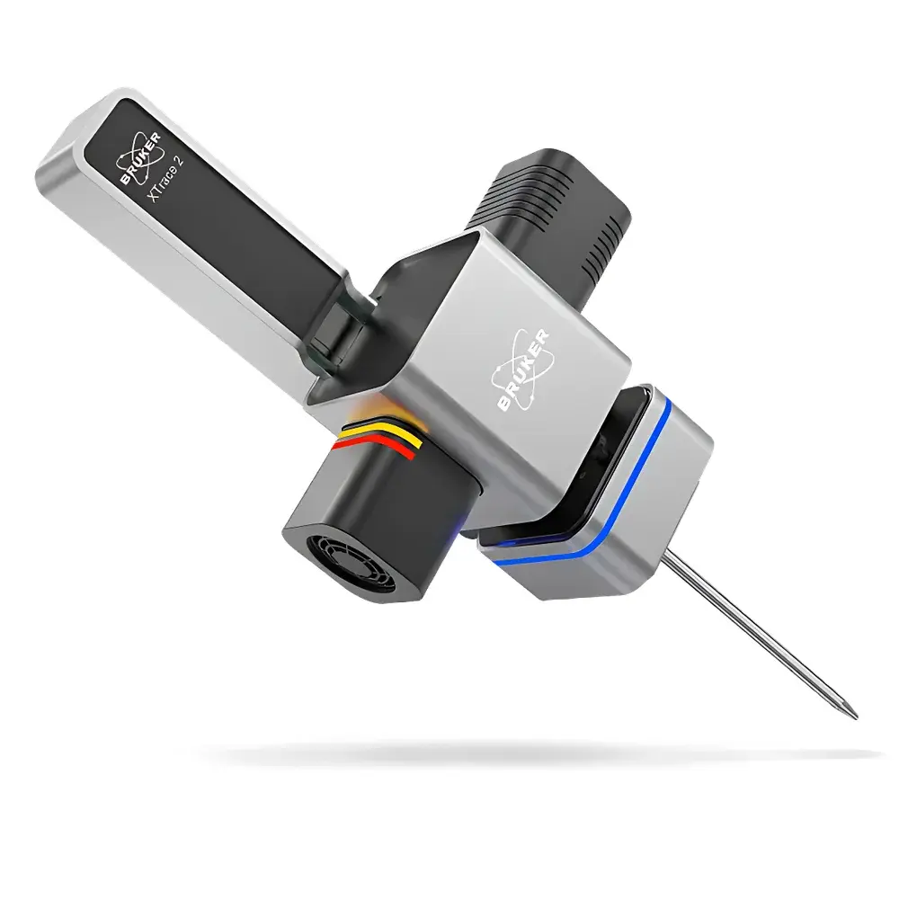
| Model | QUANTAX XTrace |
| Pricing | Available Upon Request |
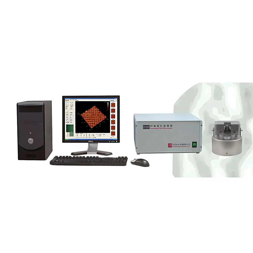
| Key | Brand: Benyuan Nanotechnology |
|---|---|
| Model | BY2000 |
| Origin | Beijing, China |
| Instrument Type | Atomic Force Microscope (AFM) / Scanning Tunneling Microscope (STM) / Lateral Force Microscope (LFM) |
| Vertical Position Detection Noise | 0.1 nm |
| Maximum Sample Diameter | 45 mm |
| Maximum Sample Thickness | 15 mm |
| XY Sample Stage Travel Range | 100 mm × 100 mm |
| XY Scan Range | ~10 μm |
| Z Scan Range | ~2 μm |
| Image Resolution Options | 128×128, 256×256, 512×512, 1024×1024 pixels |
| Scan Angle | 0–360° |
| Scan Frequency | 0.1–100 Hz |
| Controller | TI 32-bit DSP with Real-Time OS |
| DAC/ADC | 16-bit high-speed |
| High-Voltage Driver | 5-channel APEX integrated HV op-amps |
| Interface | 10/100 Mbps Fast Ethernet |
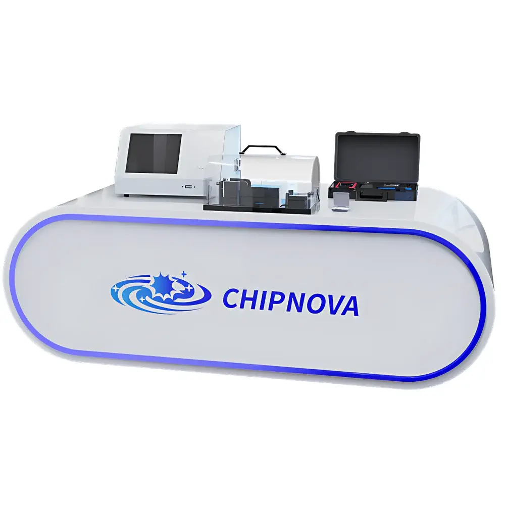
| Brand | CHIPNOVA |
|---|---|
| Origin | Fujian, China |
| Manufacturer Type | Direct Manufacturer |
| Regional Classification | Domestic (China) |
| Model | CNS-VH-LR |
| Price | USD 1.00 (Reference Only – Contact for Quotation) |
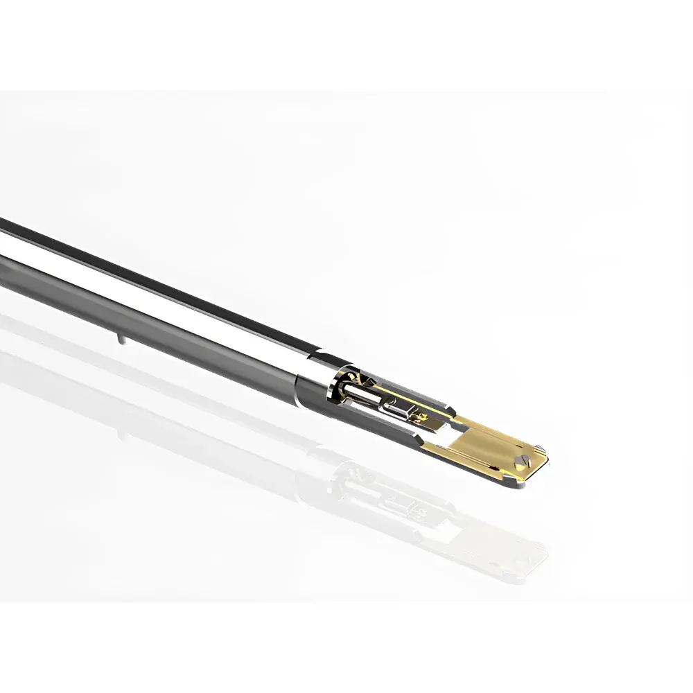
| Brand | CHIPNOVA |
|---|---|
| Origin | Fujian, China |
| Manufacturer Type | OEM Manufacturer |
| Country of Origin | Domestic (China) |
| Model | CNT-GNIH |
| Pricing | Upon Request |
| Instrument Category | In Situ Tensile/Compression Holder |
| Application Domain | Materials Science |
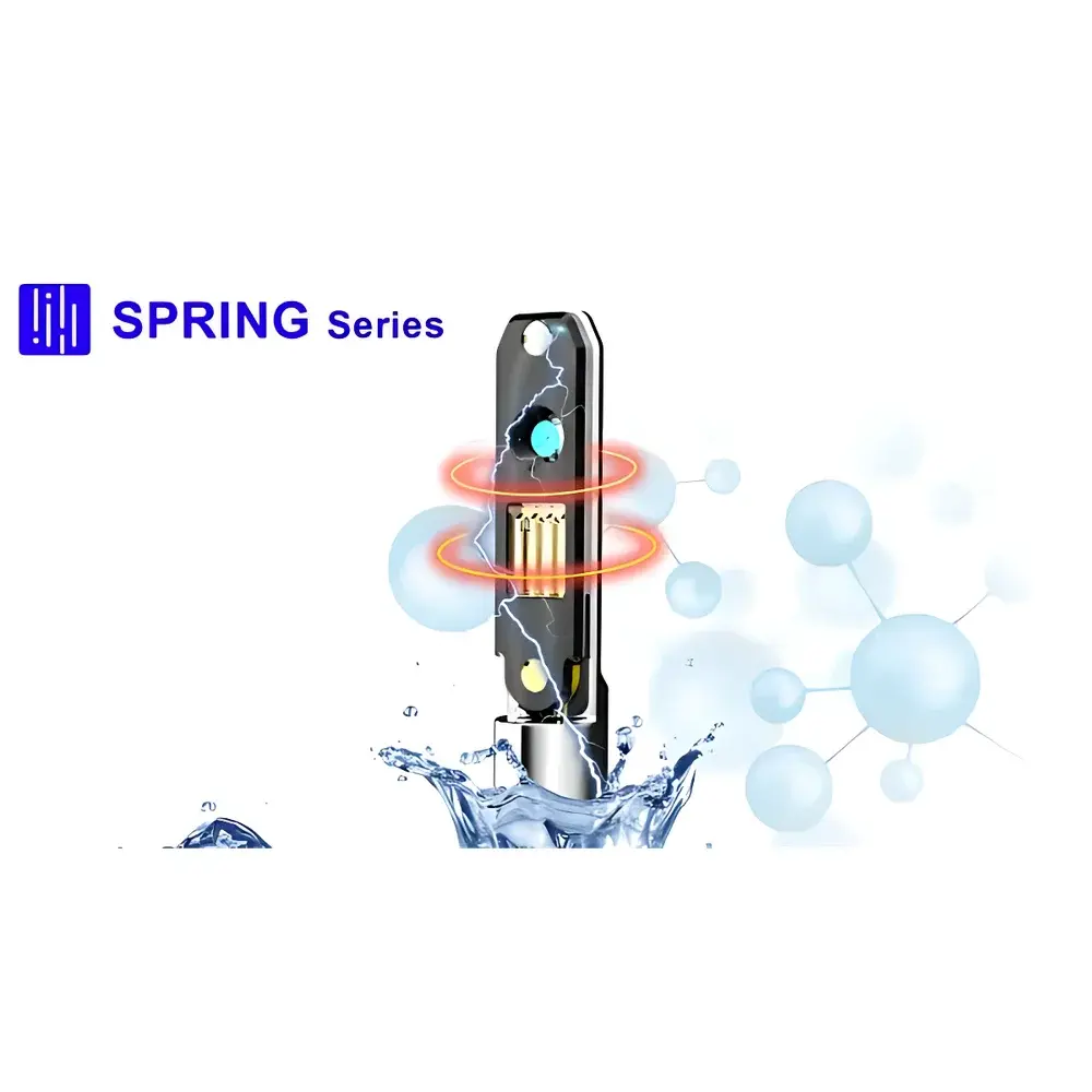
| Brand | CHIPNOVA |
|---|---|
| Origin | Fujian, China |
| Manufacturer Type | Direct Manufacturer |
| Country of Origin | China |
| Model | CNT-SHE |
| Application Category | In Situ Liquid TEM |
| Primary Application Field | Catalysis |
| Instrument Class | In Situ TEM Sample Holder |
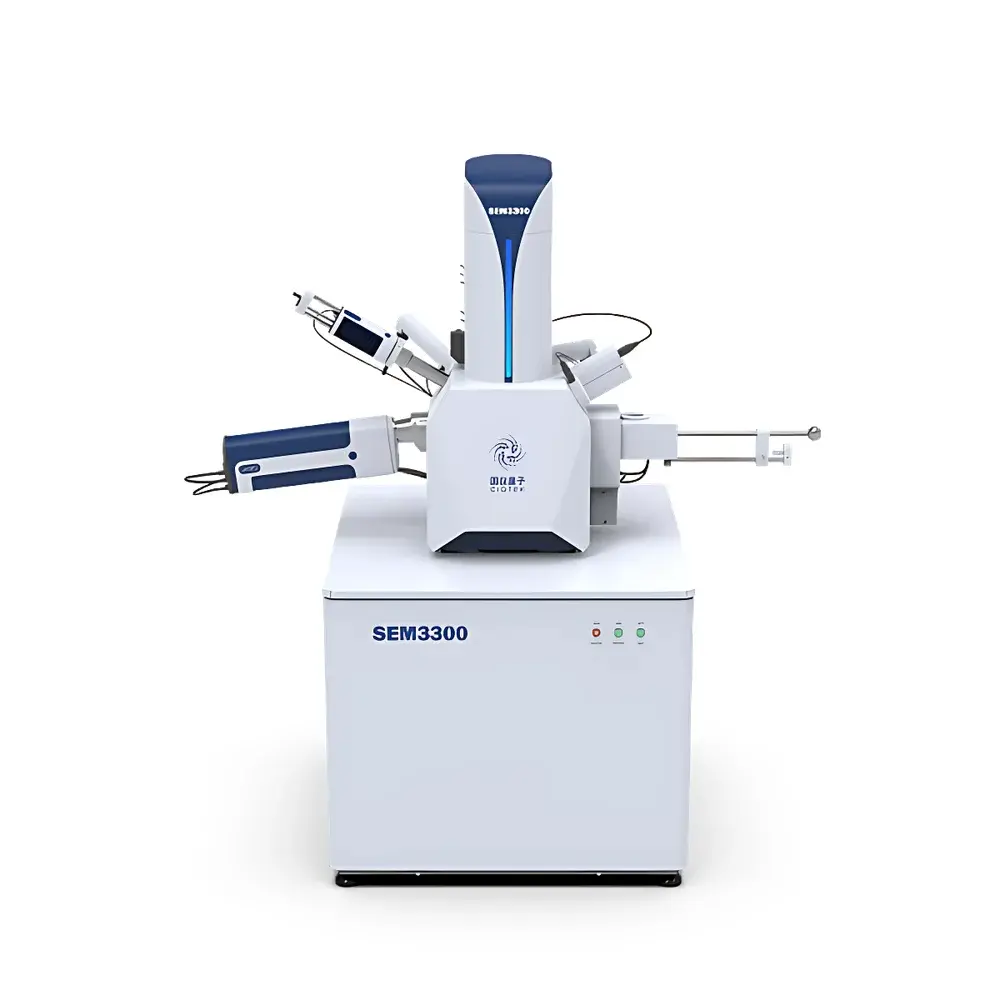
| Brand | CIQTEK |
|---|---|
| Origin | Anhui, China |
| Manufacturer Type | Direct Manufacturer |
| Origin Category | Domestic (China) |
| Model | SEM3300 |
| Instrument Type | Floor-Standing Conventional SEM |
| Electron Source | Tungsten Filament |
| SEM Class | Entry-Level Tungsten-Filament SEM |
| Secondary Electron Resolution | 2.5 nm @ 20 kV |
| Magnification Range | 1× to 300,000× |
| Accelerating Voltage | 0.1 kV to 30 kV |
| Stage Travel | X: 120 mm |
| Y | 115 mm |
| Z | 50 mm |
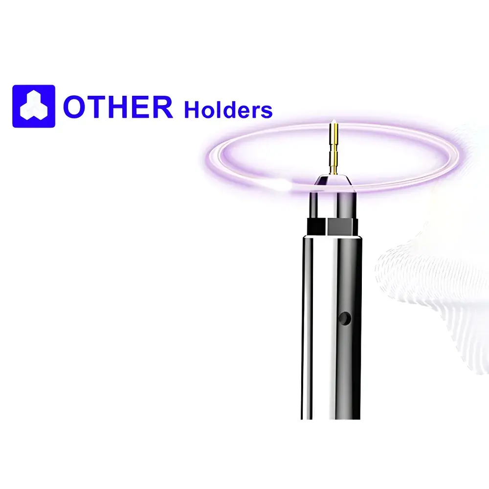
| Brand | CHIPNOVA |
|---|---|
| Model | CNT-OTAR-S |
| Holder Type | In Situ Tomographic Sample Holder |
| Compatible TEM Platforms | Thermo Fisher/FEI, JEOL, Hitachi (HR)TEM/STEM |
| Sample Mounting Options | Single-Axis Tip & C-Type Tip |
| Tip Exchangeable | Yes |
| Tip Configurations | 3 mm Half-Grid (C-Type), Rod/Conical (Single-Axis) |
| Maximum Tilt Range | ±54° (Tomographic Series) |
| Tilt Increment | 6° |
| Drift Rate | <0.5 nm/min (Stabilized State) |
| Holder Body Material | High-Strength Titanium Alloy |
| EDS/EELS/SAED Compatibility | Fully Supported |
| Application Domain | Materials Science, Nanogeology, In Situ Structural Analysis |
| Compliance | Designed for GLP-aligned electron tomography workflows |
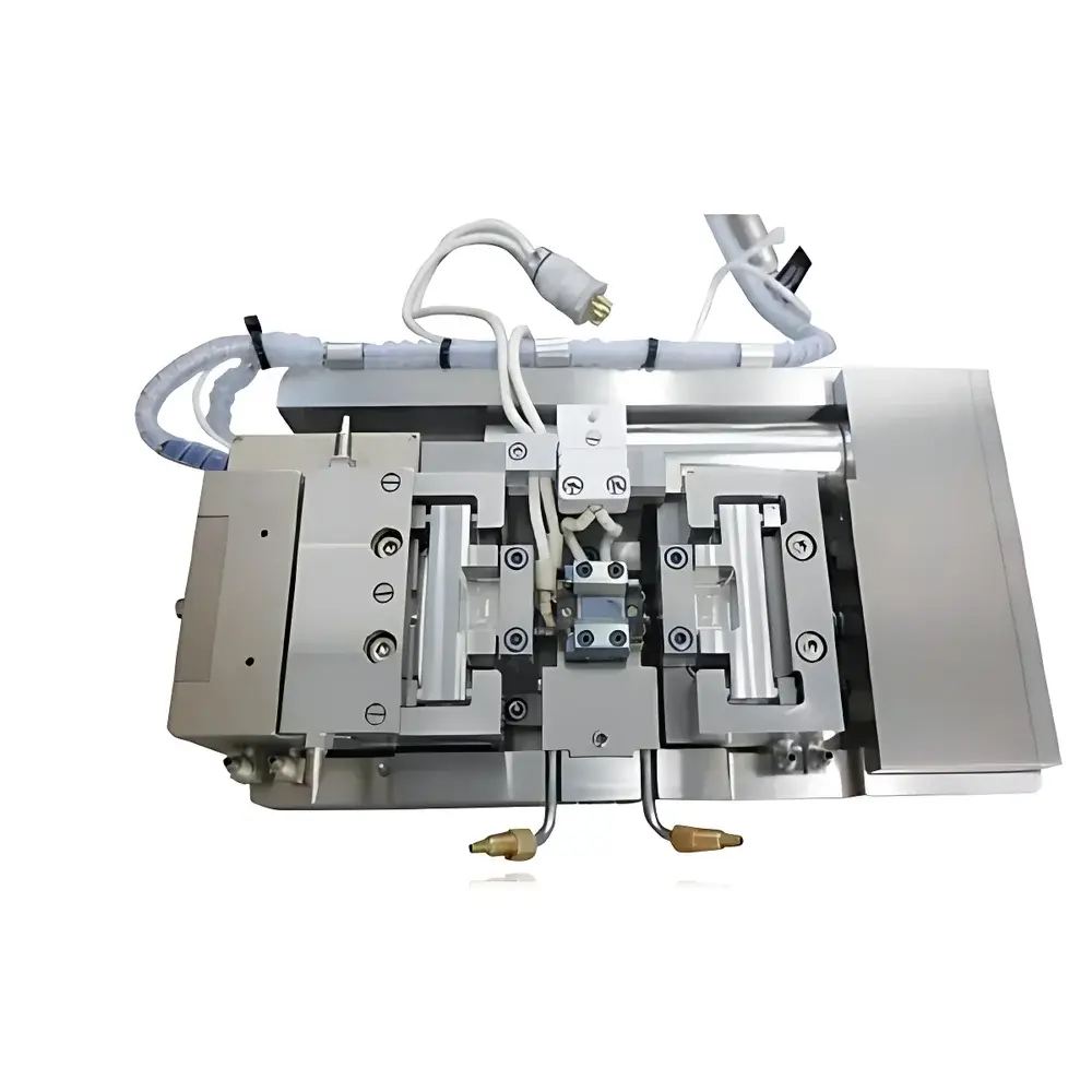
| Key | Origin: USA |
|---|---|
| Manufacturer | Deben Ltd. |
| Distributor | Optosky Co., Ltd. |
| Type | Imported |
| Model | MICROTEST |
| Load Capacity Options | 200 N, 300 N, 2000 N, 5000 N |
| Strain Rate Range | 5 µm/min – 6 mm/min |
| Force Sensor Resolution | Down to 2 N |
| Bending Configurations | Horizontal 3-point & 4-point |
| EBSD-Compatible Versions | MICROTEST2000ES/EW, MICROTEST5000S/W |
| Thermal Options | RT, Heated (EH2000/H5000), Water-Cooled (MICROTEST2000W/5000W) |
| Software | Real-time stress–strain plotting with threshold-triggered acquisition and synchronized image–data capture |
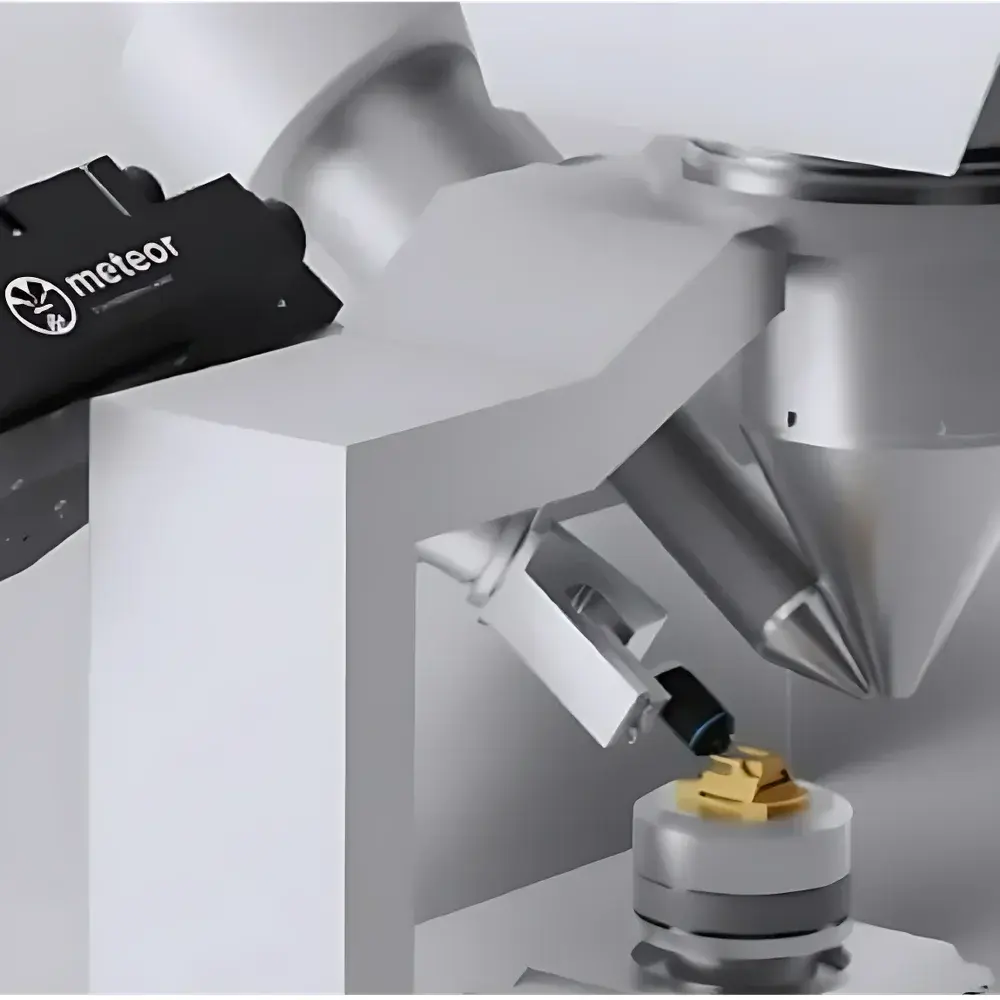
| Brand | Delmic |
|---|---|
| Origin | Netherlands |
| Model | Meteor / Meteor 2.0 |
| Integration Type | In-chamber cryo-fluorescence light microscope (cryo-FLM) for direct mounting on cryo-FIB/SEM dual-beam systems |
| Vacuum Compatibility | High-vacuum compatible (≤1×10⁻⁶ mbar) |
| Optical Resolution | Subcellular (≤300 nm lateral, dependent on NA and wavelength) |
| Field of View | Up to 500 µm × 400 µm (tile-scanned, stitched) |
| Imaging Modes | Widefield fluorescence, Z-stack acquisition, multi-channel sequential imaging |
| Excitation Sources | LED-based, configurable wavelengths (e.g., 405 nm, 488 nm, 561 nm, 640 nm) |
| Emission Filters | Motorized filter wheel with bandpass filters (FWHM ≤25 nm), minimal spectral crosstalk |
| Objective | High-NA apochromatic cryo-objective (e.g., 0.95 NA, 20× or 40×, corrected for ice thickness) |
| Detector | Back-illuminated sCMOS camera (QE >95% at 550 nm, read noise <1.5 e⁻ rms) |
| Software Platform | ODEMIS (open-source, Python-based), including ODEMIS Advanced for automated correlative workflows |
| Compliance | Designed for GLP/GMP-aligned cryo-EM workflows |
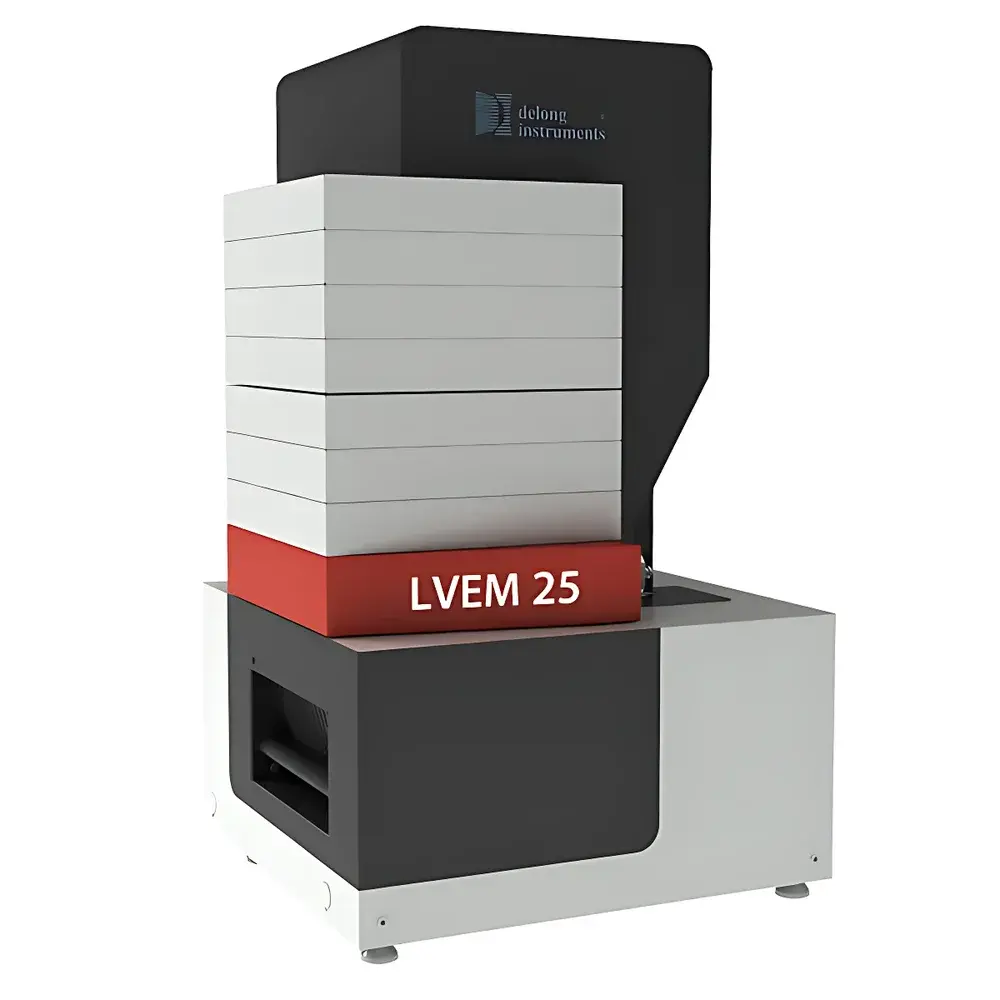
| Brand | Delong Instruments |
|---|---|
| Origin | Canada |
| Model | LVEM25 |
| Acceleration Voltages | 10, 15, 25 kV |
| Magnification Range | 1,000× – 470,000× |
| Spatial Resolution | 1 nm |
| Imaging Modes | TEM, SEM, Electron Diffraction (ED) |
| Vacuum System | Ion Pumps at Gun & Specimen Chambers |
| Electron Source | Schottky Field Emission Gun |
| Footprint | Benchtop |
| Power Requirements | Standard 120/240 V AC, No Chilled Water or Cryogens Required |