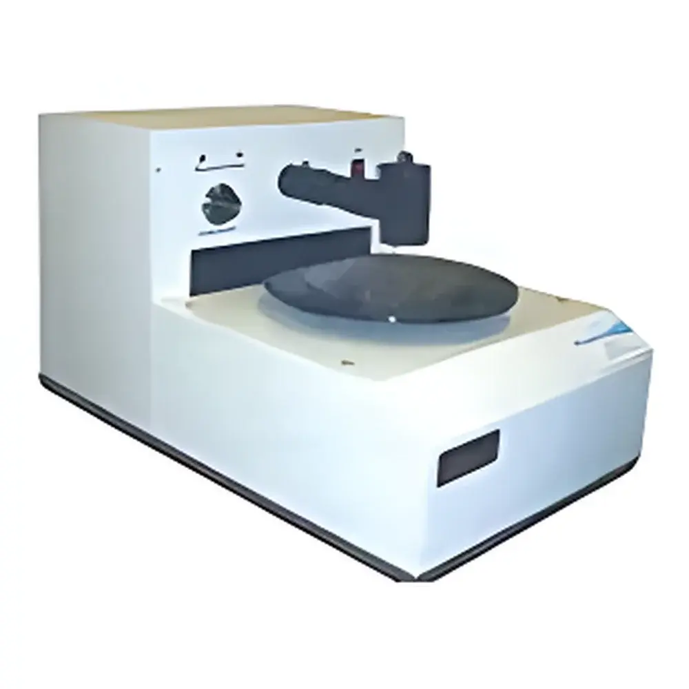
Angstrom Sun 005 Spectro-Reflectometer for Thin Film Metrology
| Origin | USA |
|---|---|
| Manufacturer Type | Authorized Distributor |
| Origin Category | Imported |
| Model | 005 |
| Pricing | Available Upon Request |
Overview
The Angstrom Sun 005 Spectro-Reflectometer is a precision optical metrology instrument engineered for non-contact, non-destructive thickness and optical constant characterization of single-layer and multi-layer thin films on planar substrates. It operates on the physical principle of spectral reflectance analysis: broadband light (UV–Vis–NIR) is incident normally or at controlled angles onto the sample surface, and the intensity distribution of reflected light across wavelength is captured by a high-resolution spectrometer. By fitting the measured reflectance spectrum to theoretical models based on Fresnel equations and layered dielectric theory, the system determines film thickness, refractive index (n), and extinction coefficient (k) with sub-nanometer resolution in thickness and <0.01 accuracy in n/k. Designed for integration into semiconductor front-end process control environments, the 005 platform supports rapid, automated measurements essential for inline process monitoring and R&D validation in IC fabrication, MEMS development, photovoltaic cell optimization, and advanced optoelectronic device manufacturing.
Key Features
- Non-destructive, contactless measurement using spectral reflectometry—no vacuum or sample preparation required
- Configurable spectral range options: standard UV–Vis (200–1000 nm), extended NIR (200–1700 nm), or custom band-limited configurations for application-specific optimization
- Thickness measurement range: 20 nm to 5000 nm for transparent and semi-transparent dielectric and conductive films—including SiO₂, Si₃N₄, photoresists, Al₂O₃, HfO₂, ITO, TiO₂, and amorphous silicon
- Automated wafer mapping capability up to 300 mm (12-inch) diameter with motorized X–Y–Z stage and integrated pattern recognition for fiducial alignment
- High-speed acquisition: full spectrum capture in 200 points/minute at 1 mm step size
- Modular optical design supporting variable angle of incidence (VASE-compatible geometry optional) and polarization-resolved measurement upgrades
Sample Compatibility & Compliance
The Angstrom Sun 005 accommodates rigid planar substrates including silicon, sapphire, quartz, glass, and metal-coated wafers from 50 mm to 300 mm in diameter and up to 2 mm in thickness. It supports both bare and patterned substrates, with software-based edge detection and mask-aware ROI definition to exclude scribe lanes or device structures during analysis. The system complies with industry-standard cleanroom requirements (ISO Class 5 compatible housing optional) and meets electromagnetic compatibility (EMC) directives per IEC 61326-1. Measurement traceability aligns with NIST-traceable calibration protocols, and data integrity features support compliance with ISO/IEC 17025, ASTM E2489-21 (Standard Guide for Spectroscopic Ellipsometry and Reflectometry), and semiconductor equipment standards SEMI E10 and E142. Audit trail and user access controls are configurable to meet GLP/GMP documentation needs.
Software & Data Management
Controlled via AngstromSun MetroSuite™ v5.x, a Windows-based application built on a modular architecture compliant with FDA 21 CFR Part 11 requirements (electronic signatures, role-based permissions, immutable audit logs). The software includes pre-loaded optical models for common film–substrate combinations, automated model selection via machine-learning-assisted fitting, and batch processing for recipe-driven measurement sequences. Raw spectra, fitted parameters, confidence metrics (χ² residuals, parameter correlation matrices), and spatial maps are stored in HDF5 format with embedded metadata (timestamp, operator ID, instrument configuration, calibration status). Export options include CSV, XML, and industry-standard SECS/GEM protocol for factory automation integration. Remote diagnostics and firmware updates are supported over secure TLS-enabled Ethernet.
Applications
- IC fab: real-time oxide/nitride gate stack verification, CMP endpoint detection, post-deposition film uniformity assessment
- MEMS: characterization of sacrificial and structural layers (e.g., SiO₂, poly-Si, Al) across device arrays
- LED & photonics: InGaN/GaN MQW layer thickness control, anti-reflection coating optimization on GaN substrates
- Solar cell R&D: transparent conductive oxide (TCO) thickness and dispersion modeling for CIGS and perovskite devices
- Display technology: ITO and metal-oxide TFT channel layer metrology on large-area glass substrates
- Research labs: optical constant databases for novel 2D materials (MoS₂, WS₂) and perovskite thin films
FAQ
What film types can the Angstrom Sun 005 measure accurately?
It measures dielectric, semiconductor, and conductive thin films—including oxides (SiO₂, Al₂O₃), nitrides (Si₃N₄), photoresists, metal oxides (ITO, ZnO), and elemental metals (Ti, Cr)—provided they exhibit measurable interference fringes in the configured spectral range.
Is calibration required before each measurement session?
A daily reference measurement on a certified Si/SiO₂ standard wafer is recommended for drift correction; full system calibration (lamp intensity, spectrometer response, stage positioning) is performed annually or after major maintenance.
Can the system integrate with existing MES or APC platforms?
Yes—MetroSuite™ supports SECS/GEM communication, OPC UA server mode, and custom REST API endpoints for bidirectional data exchange with host manufacturing execution systems.
Does the instrument require vacuum or inert atmosphere operation?
No—it operates under ambient laboratory conditions; optional nitrogen purge enclosure is available for moisture-sensitive organic films.
What level of training and technical support is provided?
Angstrom Sun offers on-site installation qualification (IQ), operational qualification (OQ), and comprehensive operator training (2-day course); global 24/7 remote support and annual preventive maintenance contracts are available.


