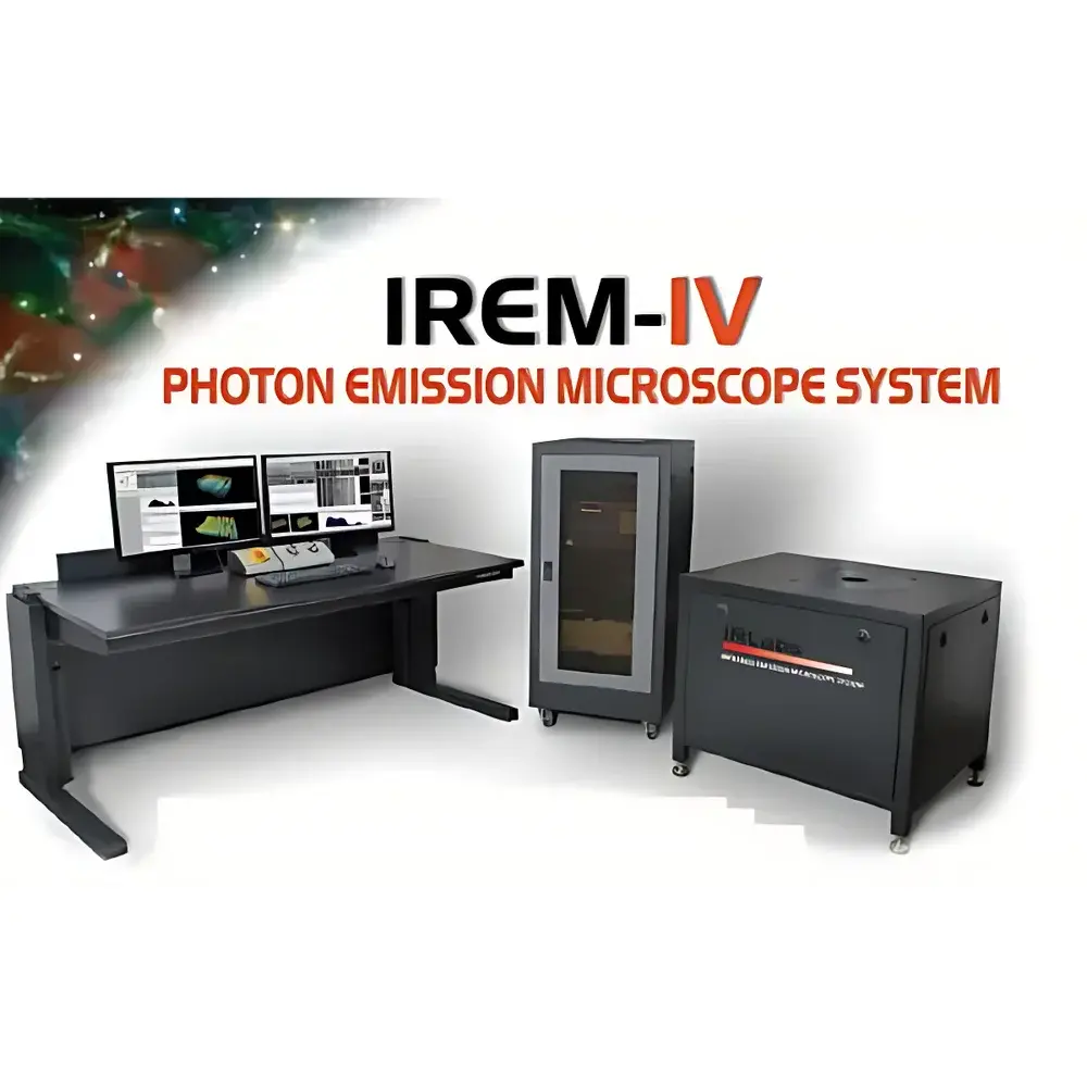
Auniontech IREM-IV Infrared Emission Microscope for Microscale Thermal Distribution Imaging
| Brand | Auniontech |
|---|---|
| Origin | Shanghai, China |
| Manufacturer Type | Authorized Distributor |
| Product Category | Domestic |
| Model | IREM-IV |
| Pricing | Upon Request |
| Camera | 1016×1016 LN₂-cooled MCT focal plane array |
| Pixel Size | 18 µm |
| Spectral Response | 400–2500 nm |
| Spatial Resolution | 25 nm (with 3.3 NA SIL objective) |
| Cooling Duration | >20 h with LN₂ dewar |
| Motion System | Motorized X-Y-Z stage (100 mm travel), tip-tilt platform with integrated contour sensor (<10 µm height resolution) |
| Objective Turret | 6-position motorized revolver |
| Filter/Wheel | Dual cryo-cooled 6-position filter & aperture wheel |
| Vibration Isolation | Active damping |
| Dimensions (Microscope) | 810 × 876 × 813 mm, 160 kg |
| Dimensions (Control Unit) | 610 × 1283 × 762 mm, 90 kg |
Overview
The Auniontech IREM-IV Infrared Emission Microscope is a high-performance, cryogenically cooled infrared imaging system engineered for non-invasive, sub-micron spatial resolution thermal emission mapping of semiconductor devices under operational bias. It operates on the principle of photon-assisted carrier recombination detection—capturing near-infrared to short-wave infrared (NIR-SWIR, 400–2500 nm) photons emitted from localized Joule heating, defect-related radiative recombination, or hot-carrier injection in active integrated circuits. Unlike conventional thermal cameras, the IREM-IV leverages liquid nitrogen–cooled mercury cadmium telluride (MCT) detector technology and solid immersion lens (SIL) optics to achieve diffraction-limited imaging at wavelengths where silicon remains transparent—enabling backside emission analysis of flip-chip packages, thinned wafers, and advanced nodes down to 10 nm process geometries. Its design prioritizes signal-to-noise ratio (SNR) optimization in photon-starved conditions typical of low-power, high-speed IC operation.
Key Features
- 1016 × 1016 pixel LN₂-cooled MCT focal plane array with 18 µm pitch, delivering ultra-low temporal and readout noise essential for single-photon-level emission detection.
- Custom 3.3 NA solid immersion lens (SIL) objective with auto-aligning, curvature-compensated tip—designed to maintain optical contact while minimizing mechanical stress on fragile die surfaces or bare wafers.
- Integrated surface contour sensor (<10 µm vertical resolution) synchronized with motorized X-Y-Z stage and tip-tilt platform, enabling real-time topographic compensation during SIL imaging.
- Dual cryo-cooled 6-position filter and aperture wheels—supporting spectral band selection (e.g., 1064 nm for OBIRCH, 1310 nm for LADA) and background suppression via pinhole apertures to mitigate thermal background noise.
- Modular optical expansion port compatible with external laser stimulation sources for time-resolved techniques including OBIRCH (Optical Beam Induced Resistance Change), LADA (Laser Assisted Device Alteration), and TIVA (Thermally Induced Voltage Alteration).
- Robust mechanical architecture featuring active vibration damping, sealed optical path, and >20-hour continuous LN₂ hold time—ensuring stability during long-duration failure localization campaigns.
Sample Compatibility & Compliance
The IREM-IV supports a broad range of semiconductor substrates and packaging configurations, including bulk silicon, SOI wafers, thinned die (≤100 µm), flip-chip BGA assemblies, and 2.5D/3D stacked ICs. Its backside imaging capability eliminates the need for decapsulation, preserving device integrity and enabling GLP-compliant failure analysis workflows. The system meets mechanical and electrical safety requirements per IEC 61000-6-2 (EMC immunity) and IEC 61010-1 (laboratory equipment safety). Data acquisition and annotation modules support audit-trail generation aligned with FDA 21 CFR Part 11 principles, facilitating integration into regulated QA/QC environments where traceability of thermal anomaly localization is required.
Software & Data Management
The IREM-IV is controlled via Auniontech’s proprietary IRVision Suite—a Windows-based application providing synchronized hardware control, real-time emission intensity mapping, multi-spectral overlay, and time-gated acquisition for transient fault capture. Image metadata (bias conditions, temperature setpoints, filter selections, stage coordinates) are embedded in TIFF and HDF5 export formats. Batch processing pipelines enable automated hotspot clustering, intensity thresholding, and correlation with CAD layout files (GDSII/OASIS import supported). All user actions—including parameter changes, image annotations, and report generation—are logged with timestamps and operator IDs, satisfying GLP/GMP documentation standards. Remote monitoring and data export via secure FTP or network-mounted storage are fully supported.
Applications
- Failure isolation in advanced logic and memory ICs—identifying leakage paths, gate oxide breakdown, and electromigration-induced hotspots.
- Dynamic power integrity analysis during functional test vectors, capturing voltage-dependent thermal transients at nanosecond-scale timing resolution.
- Process development feedback—validating thermal performance of new metallization schemes, via stacks, or FinFET channel designs.
- Reliability testing support—correlating accelerated life test (HTOL, ESD) results with localized thermal degradation signatures.
- Research in novel semiconductor materials—mapping carrier recombination dynamics in GaN HEMTs, SiC power devices, and 2D material heterostructures.
FAQ
What is the minimum detectable emission power level at 1310 nm?
The system achieves validated photon detection sensitivity equivalent to ~10⁴ photons/s at 1310 nm under 400 mV device bias—corresponding to sub-pW localized power dissipation at 10 nm node devices.
Can the IREM-IV perform time-resolved emission imaging?
Yes—when synchronized with external pulsed laser sources or digital pattern generators, the camera supports gated acquisition with adjustable delay and width down to 10 ns resolution.
Is the SIL objective compatible with oxidized or passivated wafer surfaces?
The auto-leveling, low-force SIL tip (contact force <50 mN) maintains stable optical coupling across native oxide, SiO₂, SiN, and polyimide layers without requiring index-matching fluids.
Does the system support automated defect navigation using CAD overlay?
Yes—IRVision Suite enables real-time registration of emission maps onto imported GDSII layouts with sub-micron alignment accuracy using fiducial-based coordinate transformation.
What maintenance is required for the LN₂ cooling system?
The dewar is designed for manual refill; no consumables beyond LN₂ are required. The MCT detector and optics are hermetically sealed, eliminating periodic recalibration or purge gas dependency.


