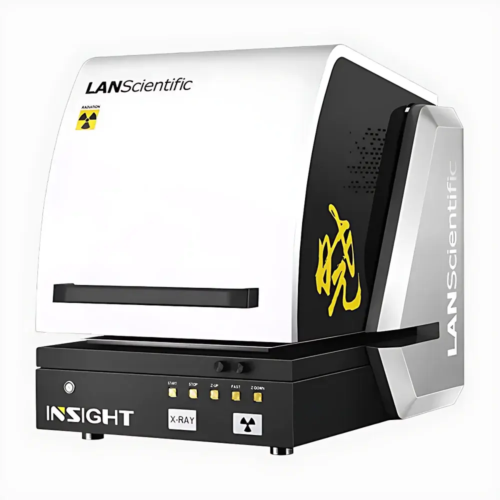
Brookfield INSIGHT PCB & Wafer Edition X-Ray Fluorescence Thickness Analyzer
| Brand | LANScientific |
|---|---|
| Origin | Jiangsu, China |
| Manufacturer Type | Direct Manufacturer |
| Regional Classification | Domestic (China) |
| Model | INSIGHT PCB & Wafer Edition |
| Pricing | Available Upon Request |
Overview
The Brookfield INSIGHT PCB & Wafer Edition is a benchtop energy-dispersive X-ray fluorescence (EDXRF) thickness analyzer engineered for non-destructive, quantitative measurement of metallic and alloy coatings on printed circuit boards (PCBs), semiconductor wafers, lead frames, connectors, and other micro-electronic substrates. Based on fundamental parameter (FP) quantification and peak deconvolution algorithms, the system measures coating thicknesses ranging from sub-nanometer to tens of micrometers with high reproducibility—without requiring matrix-matched standards. Its core architecture integrates a high-stability microfocus X-ray tube, silicon drift detector (SDD) with <125 eV Mn Kα resolution, and advanced spectral processing firmware compliant with ISO 3497 and ASTM B568 standards for electroplated and evaporated coatings.
Key Features
- Top-illumination geometry: Enables unobstructed analysis of oversized, irregular, recessed, or liquid-containing samples—including full-size PCBs (up to 400 × 300 mm), wafer carriers, and multi-height fixtures—without repositioning.
- Motorized multi-aperture collimator turret: Offers automatic switching among 8 selectable collimator sizes (25–800 µm diameter), optimizing spatial resolution and excitation efficiency per layer configuration.
- Capillary optic option: Optional polycapillary lens delivers up to 5× higher photon flux at the sample surface, enhancing detection sensitivity for ultra-thin layers (<5 nm) and low-Z elements (e.g., Ni, Cu, Sn, Pd, Au).
- Programmable XYZ motorized stage: Supports automated multi-point mapping (up to 1000 positions), line scans, and batch analysis with user-defined coordinate grids and dwell times.
- Auto-focus mechanism: Uses laser triangulation and Z-axis feedback control to maintain optimal working distance (10–80 mm) across height-varied samples—critical for warped wafers or stepped PCB features.
- C-shaped open chamber design: Provides rapid sample loading/unloading and accommodates fixtures with integrated thermal control or inert gas purging (N₂/He) for oxygen-sensitive analyses.
Sample Compatibility & Compliance
The INSIGHT PCB & Wafer Edition supports direct analysis of rigid and flexible PCBs, silicon/glass wafers (up to 300 mm diameter), lead frames, solder bumps, wire bond pads, and ENIG/ENEPIG/OSP surface finishes. It complies with ISO 3497:2022 (Metallic coatings — Measurement of coating thickness — X-ray spectrometric methods), ASTM B568–98(2022), and IPC-4552B (for ENIG thickness verification). Data integrity meets GLP/GMP requirements via audit-trail-enabled software, electronic signatures, and 21 CFR Part 11–compliant user access controls.
Software & Data Management
Powered by proprietary InsightAnalysis™ software, the system provides intuitive workflow-driven operation: one-click measurement initiation, real-time spectrum visualization, layer stack modeling (up to 5-layer configurations), and statistical reporting (Cp/Cpk, SPC charts, trend analysis). All raw spectra, calibration files, and measurement logs are stored in encrypted SQLite databases with timestamped metadata. Export formats include CSV, PDF reports (with embedded spectra), and XML-compatible outputs for LIMS integration.
Applications
- Thickness and composition verification of Au/Ni/Cu, Sn/Pb, Pd/Ni, and Ag plating on PCB edge connectors and contact fingers
- ENIG (Electroless Nickel Immersion Gold) and ENEPIG (Electroless Nickel Electroless Palladium Immersion Gold) process control in high-reliability PCB manufacturing
- Wafer-level metrology of TiW/Cu seed layers, Al/TiN gate stacks, and bump under-bump metallization (UBM)
- Lead frame plating (Ag, NiP, Sn) thickness uniformity assessment across die-attach and bond-pad regions
- Failure analysis of delamination, interdiffusion, or oxidation-induced thickness loss in multi-layer stacks
FAQ
What minimum detectable thickness can the INSIGHT achieve for gold on nickel?
For Au/Ni/Cu on FR-4, typical detection limits are ~0.3 nm Au (3σ) using capillary optics and 100 s acquisition.
Is helium purge required for light-element analysis?
Yes—He flush is recommended for reliable quantification of elements below Ti (Z=22), such as P, S, Cl, and Ca in OSP or solder mask residues.
Can the system perform multi-layer analysis without standards?
Yes—FP-based quantification enables accurate thickness determination for up to five simultaneously deposited layers without certified reference materials.
Does the software support automated pass/fail judgment against specification limits?
Yes—user-defined tolerance bands trigger color-coded alerts and auto-generate compliance summaries per IPC-A-600 or internal QC protocols.
What maintenance intervals are recommended for the X-ray tube and detector?
Tube lifetime exceeds 20,000 hours; SDD requires annual vacuum integrity verification and optional recalibration every 6 months under heavy usage.


