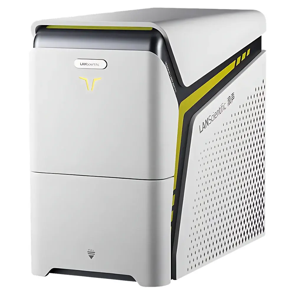
Brookfield LANScientific SuperSEM N10eX Desktop Scanning Electron Microscope with Integrated EDS
| Brand | LANScientific |
|---|---|
| Origin | Jiangsu, China |
| Manufacturer Type | Direct Manufacturer |
| Region Classification | Domestic (China) |
| Model | SuperSEM N10eX |
| Instrument Type | Desktop SEM |
| Electron Source | Tungsten Filament |
| SEM Class | Entry-Level Tungsten-Filament SEM |
| Maximum Sample Diameter | 90 mm |
| Maximum Sample Thickness | 40 mm |
| Stage Travel | X: 25 mm, Y: 25 mm, Z: 30 mm |
Overview
The Brookfield LANScientific SuperSEM N10eX is a compact, high-integration desktop scanning electron microscope engineered for routine microstructural and elemental characterization in academic laboratories, quality control facilities, and industrial R&D environments. Unlike conventional standalone SEMs, the N10eX embeds energy-dispersive X-ray spectroscopy (EDS) directly into its electron optical column architecture—enabling simultaneous acquisition of secondary electron (SE), backscattered electron (BSE), and characteristic X-ray signals during a single scan. This co-registered multimodal imaging approach leverages Coulomb-limited tungsten-filament electron optics to deliver sub-micrometer spatial resolution (<1 µm at 20 kV) while maintaining robust signal-to-noise performance across diverse non-conductive and conductive specimens. The system operates under high-vacuum conditions (base pressure ≤ 5 × 10⁻³ Pa) and supports standard accelerating voltages from 5 kV to 20 kV—optimized for balancing surface topography contrast, atomic number contrast (via BSE), and X-ray generation efficiency for quantitative EDS.
Key Features
- Integrated tungsten-filament electron column with pre-aligned condenser lens and fixed aperture—eliminating manual beam alignment and stigmator tuning during daily operation
- Real-time synchronized EDS–BSE data acquisition engine: processes spectral and imaging streams concurrently at up to 10 MHz signal bandwidth, enabling live elemental mapping without post-scan reconstruction delays
- Four-quadrant high-gain BSE detector with independent channel output and digital signal mixing—supporting compositional contrast enhancement, phase discrimination, and crystallographic orientation estimation
- Optical navigation system with integrated infrared CCD camera (640 × 480 resolution) for rapid sample positioning and chamber monitoring—reducing setup time by >60% compared to manual stage search
- Automated workflow suite: one-click auto-focus, auto-contrast/brightness, auto-stigmation, and large-area mosaic stitching (up to 100×100 tiles) with sub-pixel registration accuracy
- Compact footprint (≤ 0.8 m² floor space) and standard 220 V/50 Hz power input—requires no dedicated vibration isolation table or HVAC modifications
Sample Compatibility & Compliance
The SuperSEM N10eX accommodates specimens up to 90 mm in diameter and 40 mm in height, with motorized XYZ stage motion (25 mm × 25 mm × 30 mm travel range) supporting precise tilt-free positioning. Conductive coating (e.g., Au/Pd sputtering) is recommended for non-conductive samples; optional low-vacuum mode (optional accessory) extends usability to hydrated or outgassing-sensitive materials. All hardware and software comply with IEC 61000-6-3 (EMC emissions) and IEC 61010-1 (electrical safety). Data handling workflows support audit-trail logging per GLP/GMP requirements, and EDS quantification routines follow ISO 16700:2016 (microanalysis — quantification procedures for EDS) and ASTM E1508–22 (standard guide for quantitative analysis by EDS).
Software & Data Management
The proprietary SuperSEM Suite v4.x provides a unified interface for instrument control, real-time imaging, spectral acquisition, and offline quantification. Key modules include: Live EDS Mapping (pseudo-color elemental overlays updated at ≥15 fps), Spectrum Library Manager (with NIST Standard Reference Database integration), Peak Deconvolution Engine (based on iterative least-squares fitting), and Report Generator compliant with ISO/IEC 17025 documentation standards. Raw data (including .ser, .eds, .tif stacks) are stored in vendor-neutral HDF5 format with embedded metadata (voltage, working distance, dwell time, detector geometry). Software supports 21 CFR Part 11-compliant user authentication, electronic signatures, and immutable audit trails for regulated environments.
Applications
- Materials Science: Phase identification in alloys, intermetallic distribution in battery cathodes (e.g., NMC, LFP), coating thickness measurement via cross-section BSE imaging
- Geosciences: Mineral assemblage mapping in thin sections, porosity analysis in cementitious matrices using SE/BSE dual-mode segmentation
- Life Sciences: Cell morphology assessment on conductive substrates, elemental localization in calcified tissues (Ca/P ratio mapping)
- Forensics: Gunshot residue (GSR) particle classification (Sb/Ba/Pb signature), fiber trace evidence comparison via morphology + EDS fingerprinting
- Electronics: Solder joint void detection, Cu diffusion analysis in PCB laminates, failure root-cause attribution via localized Cl/Na contamination mapping
FAQ
Does the SuperSEM N10eX require liquid nitrogen cooling for the EDS detector?
No—the integrated silicon drift detector (SDD) uses Peltier thermoelectric cooling to maintain optimal operating temperature (−20 °C), eliminating cryogen dependency and enabling continuous duty-cycle operation.
Can the system perform quantitative EDS analysis without standards?
Yes—ZAF and φ(ρz) matrix correction models are embedded, and standardless quantification is validated against certified reference materials (e.g., NIST SRM 2782, 2783) with typical relative errors 1 wt%).
Is remote operation supported?
Yes—secure WebSocket-based remote access allows full instrument control and data review via browser on Windows/macOS/Linux, with TLS 1.2 encryption and role-based permission management.
What vacuum maintenance is required?
The turbomolecular pump is rated for 20,000 hours MTBF; oil-free scroll backing pump requires only annual filter replacement. System includes automated vacuum diagnostics and leak-rate trending logs.
How is beam damage mitigated for beam-sensitive polymers?
Low-kV imaging (5–10 kV), reduced probe current (<100 pA), and frame-averaged video mode minimize charging and decomposition—validated on PMMA, PVDF, and biological hydrogels.


