Bruker AFM Probes for Atomic Force Microscopy
| Brand | Bruker |
|---|---|
| Origin | USA |
| Product Type | AFM Cantilever Probes |
| Material | Single-Crystal Silicon or Silicon Nitride |
| Tip Radius | 1 nm – 30 nm (model-dependent) |
| Spring Constant | 0.25 N/m – 450 N/m |
| Resonant Frequency | 10 kHz – 525 kHz |
| Coating Options | Al, Au, PtIr, Cr/Au, Conductive Diamond, DLC, Magnetic CoCr, Ptlr |
| Packaging | Individual Box (10 pcs), Wafer (300–400 pcs), or Custom Sets |
| Compliance | ISO/IEC 17025 traceable calibration available for certified probes |
Overview
Bruker AFM Probes are precision-engineered cantilever sensors designed exclusively for integration with Bruker’s Dimension™, Icon™, FastScan™, and Innova™ atomic force microscopes. These probes operate on the fundamental principle of nanomechanical deflection sensing: a sharp tip mounted on a microfabricated cantilever interacts with sample surfaces via van der Waals, electrostatic, magnetic, or capillary forces; resulting cantilever bending or oscillation is detected optically (laser beam deflection) or piezoresistively to reconstruct topographic, mechanical, electrical, or magnetic properties at sub-nanometer resolution. As consumable components critical to measurement fidelity, probe performance directly governs signal-to-noise ratio, spatial resolution, imaging stability, and quantitative reproducibility—particularly in dynamic modes such as tapping, PeakForce Tapping®, and contact-mode force spectroscopy. All Bruker probes undergo rigorous post-fabrication metrology—including tip radius verification via TEM, spring constant calibration per Sader or thermal noise methods, and resonance frequency validation—ensuring consistency across batches and compatibility with GLP/GMP-compliant workflows.
Key Features
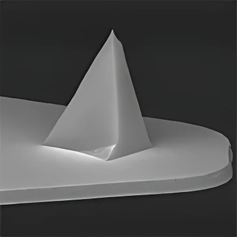
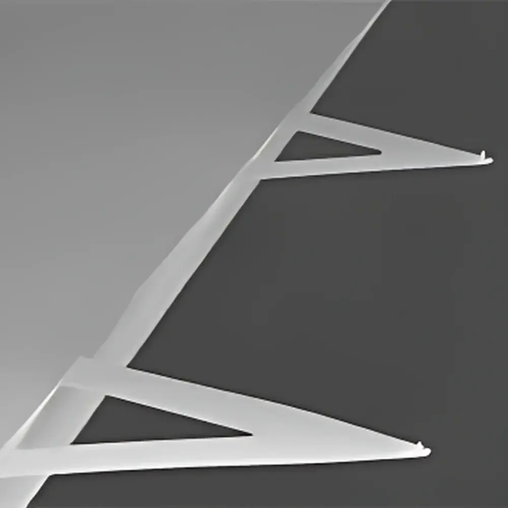
- Material & Fabrication: High-purity monocrystalline silicon or low-stress silicon nitride substrates, fabricated using photolithography and deep reactive ion etching (DRIE) for dimensional accuracy and batch uniformity.
- Tip Geometry Control: Nominal tip radii ranging from 1 nm (e.g., PEAKFORCE-HiRs-SSB, SAA-HPI-SS) to 30 nm (e.g., RTESPA-150-30), with certified end-radius options for quantitative nanomechanics (QNM) and PeakForce QNM®.
- Coating Versatility: Backside aluminum for optical reflectivity enhancement; front-side conductive coatings (PtIr, PtSi, Cr/Au, Ptlr) for KPFM, EFM, SCM, and C-AFM; magnetic CoCr layers for MFM; diamond-like carbon (DLC) or conductive diamond for wear resistance in harsh environments.
- Mode-Specific Optimization: Dedicated probe families engineered for distinct operational regimes—SCANASYST® for automated intelligent imaging; FASTSCAN® for high-speed scanning (>1 Hz frame rate); PFQNE-AL for Kelvin probe force microscopy; DDESP-V2 for piezoresponse force microscopy (PFM); SSRM-DIA for scanning spreading resistance microscopy.
- Calibration-Ready Options: Pre-certified probes (e.g., RTESPA-150-30, SAA-HPI-30) include NIST-traceable spring constants and controlled tip geometry, eliminating in-lab calibration uncertainty and supporting audit-ready documentation per FDA 21 CFR Part 11 requirements.
Sample Compatibility & Compliance
Bruker AFM probes support operation across ambient air, liquid (aqueous and organic solvents), vacuum, and temperature-controlled stages (–30 °C to +200 °C). Probe selection is rigorously mapped to sample mechanical properties: soft biological specimens (cells, proteins, polymers) require low-k cantilevers (<1 N/m, e.g., SCANASYST-FLUID+, DNP-10); stiff inorganic materials (metals, ceramics, semiconductors) demand high-k probes (≥40 N/m, e.g., RTESPA-300, AD-40-AS); nanomechanical indentation uses ultra-high-k diamond-tipped probes (DNISP-HS, 450 N/m). All probes comply with ISO 18473-3 (nanomaterials characterization) and ASTM E2531 (AFM probe calibration standards). For regulated industries, probe lot traceability, certificate of conformance, and optional ISO/IEC 17025-accredited calibration reports are provided.
Software & Data Management
Probe metadata—including nominal k-value, f0, tip radius, coating type, and packaging configuration—is embedded in Bruker’s NanoScope® software via probe recognition tags. This enables automatic parameter loading during mode setup, reducing operator error and ensuring repeatable acquisition protocols. The NanoScope Analysis platform supports quantitative force curve fitting (Hertz, Sneddon, DMT models), modulus mapping, and statistical reporting aligned with ASTM E2926 and ISO 14573. Audit trails record probe usage history, calibration status, and environmental conditions—essential for 21 CFR Part 11 compliance in pharmaceutical QC and medical device R&D.
Applications
- Materials Science: Grain boundary analysis in battery cathodes, polymer phase separation, graphene layer counting, and thin-film adhesion quantification.
- Life Sciences: Live-cell morphology under physiological buffer, amyloid fibril stiffness mapping, DNA-protein binding kinetics, and membrane protein clustering via high-speed FASTSCAN®.
- Semiconductor Metrology: Critical dimension (CD) verification, gate oxide thickness profiling, and dopant distribution imaging via SSRM and SCM.
- Electrochemistry: In-situ SECM-AFM hybrid studies of electrode/electrolyte interfaces, corrosion pit nucleation, and solid-electrolyte interphase (SEI) evolution.
- Nanomechanics: Local Young’s modulus extraction (1 MPa–10 GPa range), viscoelastic relaxation time constants, and creep compliance modeling using QNM and PF-QNM®.
FAQ
How do I select the correct probe for my application?
Begin by identifying your primary measurement objective (topography, conductivity, magnetism, mechanics), sample environment (air/liquid/vacuum), and mechanical properties (soft/hard). Then match to Bruker’s mode-specific families—e.g., SCANASYST-AIR for routine air imaging, FASTSCAN-D for live-cell dynamics, or PFQNE-AL for surface potential mapping.
Are Bruker probes compatible with non-Bruker AFM systems?
Yes—many series (e.g., RTESPA, SNL, MLCT, TESP) follow standard 500 µm × 50 µm chip dimensions and are mechanically compatible with Park Systems, Asylum Research, and JPK instruments. However, full software integration and automated calibration require Bruker hardware and NanoScope control.
What does “-A”, “-W”, or “-SS” signify in probe model numbers?
“-A” denotes a 10-probe box with Al-coated backside; “-W” indicates a wafer-packaged set (~300–400 probes) without coating; “-SS” specifies an ultra-sharp tip (≤2 nm radius) optimized for high-resolution imaging.
Do you provide calibration certificates for quantitative work?
Yes—certified probes (e.g., RTESPA-150-30, SAA-HPI-30) ship with ISO/IEC 17025-accredited calibration data including measured k-value, tip radius, and resonant frequency, traceable to NIST standards.
Can I use the same probe for both topography and electrical measurements?
Only if explicitly designed for multimodal operation—e.g., SCM-PIT-V2 combines conductive PtIr coating with calibrated mechanical properties for simultaneous topography and current mapping. Standard topographic probes lack electrical functionality and may introduce artifacts in EFM/KPFM.


