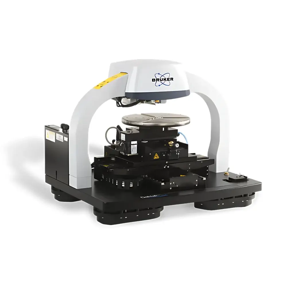
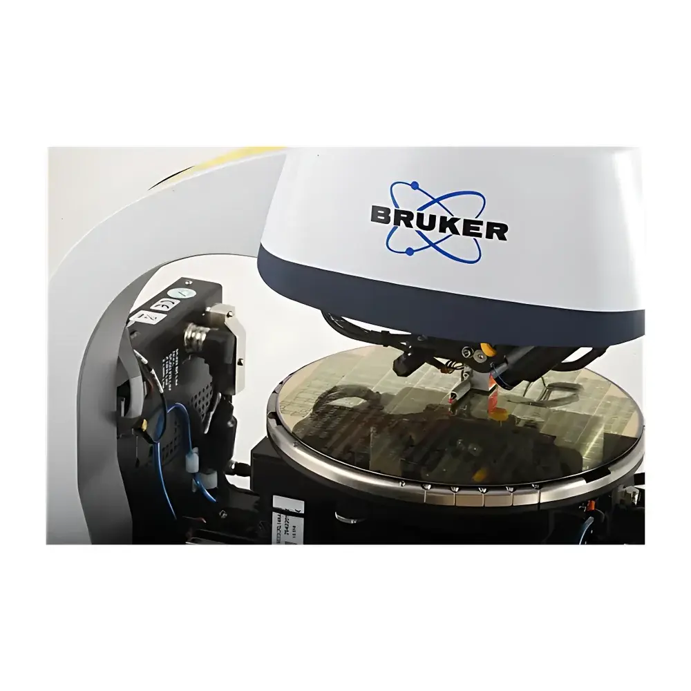
Bruker Dektak Pro Stylus Profilometer
| Brand | Bruker |
|---|---|
| Origin | USA |
| Model | Dektak Pro |
| Type | Contact Stylus Profilometer |
| Operating Principle | Mechanical Stylus Scanning (Tactile Profilometry) |
| Category | Precision Geometric Measurement Instrument |
Overview
The Bruker Dektak Pro is a high-performance contact stylus profilometer engineered for nanoscale vertical resolution and sub-micron lateral repeatability in surface topography characterization. It operates on the fundamental principle of mechanical stylus scanning: a diamond-tipped probe (typically 2–12.5 µm radius) traverses the sample surface under controlled force (0.3–15 mg), converting vertical displacement into analog voltage via a linear variable differential transformer (LVDT) sensor. This analog signal is digitized with 16-bit resolution and processed to generate quantitative height profiles, step heights, roughness parameters (e.g., Ra, Rq, Rz per ISO 4287/ISO 25178), and cross-sectional area metrics. Designed for laboratory and production environments requiring traceable, NIST-calibratable measurements, the Dektak Pro delivers robust performance across semiconductor process control, thin-film metrology, and advanced materials R&D—without reliance on optical interference or laser scatter assumptions.
Key Features
- High-sensitivity LVDT-based transduction system enabling <1 Å vertical resolution (RMS) and <0.1 nm noise floor over 1 Hz bandwidth
- Motorized Z-stage with 1 mm travel range and closed-loop feedback for precise touchdown control and automated multi-point measurement routines
- Programmable stylus force from 0.3 mg to 15 mg, optimized for soft polymers, brittle oxides, and hard metallic films
- Scan lengths up to 100 mm with 0.1 µm lateral positioning accuracy (stepper motor + encoder feedback)
- Integrated environmental isolation: vibration-damped granite base and optional acoustic enclosure for low-noise operation
- Modular design supporting interchangeable stylus holders, extended-range Z-sensors, and vacuum-compatible stages (optional)
Sample Compatibility & Compliance
The Dektak Pro accommodates substrates ranging from 10 mm × 10 mm wafers to full 300 mm silicon wafers (with optional chuck), as well as irregularly shaped samples up to 200 mm in diameter and 50 mm in height. It supports rigid and semi-rigid materials including Si, SiO₂, SiN, metals (Al, Cu, Ti), photoresists, spin-on glass, polymer coatings (e.g., PMMA, SU-8), biomedical hydrogels, and MEMS devices. All measurements comply with ISO 25178-2 (areal surface texture), ISO 4287 (profile-based roughness), ASTM E1093 (stylus profilometry standard practice), and USP for pharmaceutical film thickness verification. The system architecture meets GLP/GMP documentation requirements, including full audit trail logging, user access control, and electronic signature support aligned with FDA 21 CFR Part 11 when configured with Bruker’s Compass software suite.
Software & Data Management
Bruker Compass is the native acquisition and analysis platform for the Dektak Pro, offering intuitive workflow-driven operation—from single-line profiling to automated grid mapping and multi-layer stack analysis. It provides real-time filtering (Gaussian, Spline, Robust Gaussian), ISO-compliant roughness parameter calculation (Ra, Rq, Rsk, Rku, Rz, Rpc), step-height deconvolution using edge detection algorithms, and film-thickness modeling for transparent overlays (e.g., SiO₂ on Si). Data export supports CSV, ASCII, .sur, and .stp formats; integration with MATLAB, Python (via Bruker SDK), and LabVIEW enables custom automation and statistical process control (SPC) deployment. Raw data files are timestamped, checksum-verified, and stored with full metadata (probe ID, force setting, scan speed, environment log), ensuring full traceability for QA/QC audits.
Applications
- Semiconductor & MEMS: Etch depth uniformity across wafer maps, CMP endpoint detection, TSV sidewall profile assessment, and lithographic resist thickness validation
- Optical & Decorative Coatings: UV-curable lens coatings, PVD-deposited decorative finishes on faucets, and anti-reflective multilayer stacks on AR/VR optics
- Thin-Film & Energy Devices: Thickness and interfacial roughness of perovskite layers in solar cells, solid-electrolyte interfaces in solid-state batteries, and ALD-grown barrier films
- Life Sciences & Microfluidics: Quantification of PDMS channel depth post-molding, surface topography of biofunctionalized sensor chips, and thickness gradients in electrospun nanofiber mats
- Quality Assurance: In-line process monitoring for roll-to-roll coated films, batch release testing of medical device coatings (ISO 10993-1), and supplier qualification per IATF 16949 requirements
FAQ
What stylus tip radius options are available for the Dektak Pro?
Standard configurations include 2 µm, 5 µm, and 12.5 µm diamond tips; custom radii (e.g., 0.5 µm or 25 µm) are available upon request.
Can the Dektak Pro measure transparent or highly reflective surfaces?
Yes—unlike optical profilers, contact stylus measurement is independent of optical properties; no special preparation (e.g., antireflective coating) is required.
Is thermal drift compensation built into the system?
The Dektak Pro features an internal temperature sensor and real-time Z-axis offset correction algorithm, reducing thermal drift to <0.5 nm/°C over 8-hour operation.
How is calibration performed and maintained?
Traceable step-height standards (e.g., NIST SRM 2155) are used for periodic verification; Compass software includes automated calibration routines with pass/fail reporting per ISO/IEC 17025 guidelines.
Does the system support automated wafer handling?
Yes—integrated robotic interface (SEMI E47 compliant) and wafer alignment vision module are available as factory-installed options for high-throughput fabs.