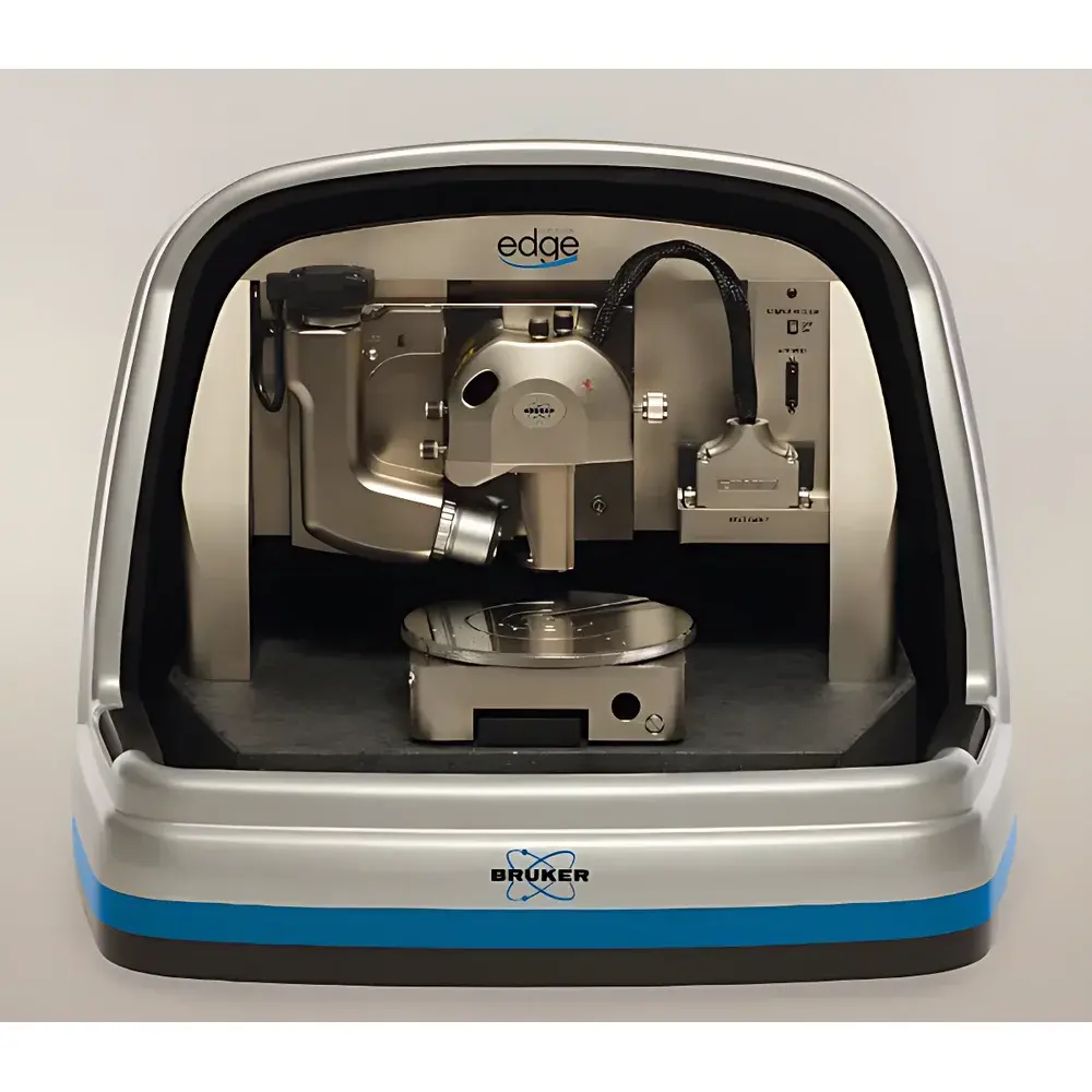
Bruker Dimension Edge Atomic Force Microscope
| Brand | Bruker |
|---|---|
| Origin | USA |
| Model | Dimension Edge |
| Instrument Type | Material-Focused AFM |
| Positioning Noise | X-Y ≤ 50 pm RMS, Z ≤ 50 pm RMS |
| Sample Diameter | 150 mm (vacuum chuck), Thickness: ≤ 15 mm |
| Scan Area | 150 mm × 150 mm |
| Imaging Bandwidth | Typical high-speed acquisition capability |
| Category | Scanning Probe Microscope (SPM) / Atomic Force Microscope (AFM) |
Overview
The Bruker Dimension Edge Atomic Force Microscope is a high-performance, closed-loop scanning AFM engineered for nanoscale metrology across diverse material science, semiconductor, polymer, and life science applications. Built upon the proven architecture of the Dimension Icon® platform, the Dimension Edge integrates Bruker’s proprietary low-noise sensor design, FPGA-based thermal drift compensation, and a rigid bridge-mounted scanner to deliver sub-angstrom stability and resolution—traditionally achievable only on small-sample, open-loop systems—while supporting large-area samples up to 150 mm in diameter. Its operational principle relies on piezoelectric actuation combined with integrated capacitive position sensing for real-time feedback control, enabling true closed-loop imaging without sacrificing signal-to-noise ratio. This architecture ensures quantitative topographic fidelity, minimal thermal drift (<0.5 nm/h under ambient conditions), and high reproducibility essential for GLP-compliant surface characterization and ISO/IEC 17025 traceable measurements.
Key Features
- True closed-loop scanning with capacitive position sensors delivering X-Y ≤ 50 pm RMS and Z ≤ 50 pm RMS noise performance
- Rigid bridge structure with active temperature stabilization for ultra-low thermal drift (sub-nanometer/hour stability)
- 150 mm × 150 mm motorized sample stage with programmable navigation and 5-megapixel optical microscope for rapid region-of-interest targeting
- Modular, low-noise electronics architecture supporting simultaneous multi-channel signal acquisition and real-time signal routing
- Intuitive workflow-driven software interface with guided setup, automated calibration routines, and context-aware parameter optimization
- Patented Dark Lift™ mode for unambiguous separation of photogenerated current from intrinsic conductivity in electro-optical materials
- Native support for dual-frequency electrostatic force microscopy (EFM), scanning capacitance microscopy (SCM), and Kelvin probe force microscopy (KPFM)
Sample Compatibility & Compliance
The Dimension Edge accommodates a broad range of sample geometries and environments: flat or mildly curved substrates up to 150 mm in diameter and 15 mm thick, secured via vacuum chuck. It supports ambient, inert gas, and controlled-humidity operation without modification. The system complies with international standards relevant to nanometrology instrumentation, including ISO 25178-601 (areal surface texture parameters), ASTM E2531 (standard guide for AFM calibration), and USP (instrument qualification for pharmaceutical surface analysis). Data integrity features—including full audit trail, electronic signatures, and 21 CFR Part 11–compliant user access controls—are available through optional Bruker NanoScope Analysis software modules, meeting GMP/GLP laboratory requirements for regulated research.
Software & Data Management
Powered by Bruker’s latest NanoScope 8 software suite, the Dimension Edge provides a unified environment for acquisition, visualization, quantification, and reporting. The software includes over 30 preconfigured AFM modes—from contact and tapping to PeakForce Tapping®, Conductive AFM, and Piezoresponse Force Microscopy—with customizable scripting via Python API. All raw data are stored in vendor-neutral HDF5 format with embedded metadata (scan parameters, calibration constants, timestamp, user ID), ensuring long-term accessibility and FAIR (Findable, Accessible, Interoperable, Reusable) data principles. Batch processing workflows, spectral analysis tools, and statistical surface roughness calculators conform to ISO 4287 and ISO 25178 standards. Export options include TIFF, PNG, CSV, and MATLAB-compatible formats for third-party analysis integration.
Applications
The Dimension Edge serves as a versatile platform for quantitative nanoscale characterization across multiple domains: semiconductor device inspection (gate oxide thickness, dopant profiling via SCM), photovoltaic material analysis (grain boundary mapping, phase segregation in perovskites), advanced polymer morphology (crystallinity, block copolymer domain spacing), and biological sample imaging (intact cells, membrane proteins, extracellular vesicles) under near-physiological conditions. Its Dark Lift™ capability enables definitive charge separation studies in organic photodetectors and perovskite solar cells. In failure analysis labs, the system supports cross-sectional AFM, nanomechanical property mapping (elastic modulus, adhesion), and time-resolved electrical spectroscopy—all within a single platform. Academic and industrial users routinely publish Dimension Edge data in journals such as *ACS Nano*, *Advanced Materials*, and *Nature Communications*.
FAQ
What distinguishes Dimension Edge from open-loop AFMs?
It combines closed-loop positional accuracy with open-loop noise performance through patented sensor design and FPGA-based thermal compensation—enabling both high-resolution imaging and large-area metrology.
Can Dimension Edge perform electrical measurements under vacuum or inert atmosphere?
Yes; the instrument supports optional environmental chambers and is compatible with low-current preamplifiers (fA-level sensitivity) for conductive, piezoelectric, and electrochemical AFM modes in controlled environments.
Is NanoScope 8 software compatible with legacy Bruker AFM data files?
Yes; NanoScope 8 maintains full backward compatibility with all prior NanoScope file formats (.spm, .msr) and provides automated metadata migration and batch reprocessing tools.
Does the system meet regulatory requirements for quality-controlled laboratories?
With optional validation packages and 21 CFR Part 11–enabled software modules, it supports IQ/OQ/PQ documentation, audit trails, and role-based access control for GMP/GLP compliance.
How is sample navigation optimized for large substrates?
Integrated 5 MP optical imaging, motorized XYZ stage with 150 mm travel, and pattern-recognition–assisted coordinate linking enable precise multi-site measurement across wafers or tissue sections without manual repositioning.


