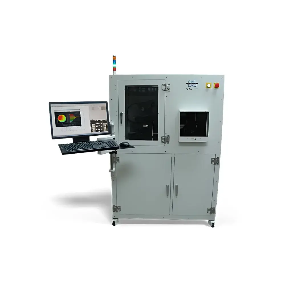
Bruker FilmTek 2000 PAR-SE Spectroscopic Ellipsometer with Multi-Angle Differential Polarimetry and Extended DUV-NIR Range
| Brand | Bruker |
|---|---|
| Origin | Germany |
| Model | FilmTek 2000 PAR-SE |
| Spectral Range | 190 nm – 1700 nm |
| Spot Size | 25 µm – 300 µm |
| Measurement Speed | <1 second per site |
Overview
The Bruker FilmTek 2000 PAR-SE is a high-precision, multi-mode spectroscopic ellipsometer engineered for quantitative thin-film metrology across R&D, pilot-line development, and high-volume semiconductor manufacturing environments. It operates on the physical principle of spectroscopic ellipsometry—measuring the change in polarization state of light upon reflection from a sample surface—to extract complex optical constants (n(λ), k(λ)) and geometric parameters (layer thicknesses, roughness, grading, void fraction) with sub-Å resolution. Its PAR-SE architecture integrates three complementary optical measurement modalities: (1) rotating-compensator spectroscopic ellipsometry (RC-SE) from 295 nm to 1700 nm; (2) multi-angle polarized spectroscopic reflectometry (MAPR) covering 190–1700 nm, including deep-ultraviolet (DUV); and (3) proprietary Multi-Angle Differential Polarimetry (MADP) combined with Differential Power Spectral Density (DPSD) analysis. This fusion enables robust characterization of ultra-thin native oxides (<10 Å), compositionally graded layers, anisotropic materials (e.g., strained SiGe), and patterned wafers—where conventional single-mode instruments exhibit reduced sensitivity or model ambiguity.
Key Features
- Simultaneous determination of thickness, refractive index n(λ), extinction coefficient k(λ), bandgap, composition (e.g., Ge% in Si1−xGex, Al% in AlxGa1−xAs), surface roughness, crystallinity (amorphous vs. polycrystalline), and vertical compositional gradients.
- Extended spectral coverage from 190 nm (DUV) to 1700 nm (NIR), enabled by a regulated deuterium-halogen lamp and dual-detector configuration: 2048-pixel Sony linear CCD (UV-VIS-NIR) and cooled 512-pixel Hamamatsu InGaAs CCD (NIR).
- Variable spot size from 25 µm to 300 µm at normal incidence (2 mm at 70°), supporting both high-resolution micro-spot mapping and macro-area averaging.
- Integrated Cognex vision system with pattern recognition for automated alignment and coordinate-based measurement on patterned wafers and product die.
- Parabolic mirror optical design minimizing aberrations and maximizing throughput and signal-to-noise ratio across the full spectral range.
- Automated motorized stage (300 mm travel) with autofocus capability and wafer handling compatibility for FOUP and SMIF carriers per SEMI standards.
- Advanced Bruker FilmTek software featuring global optimization algorithms, generalized material models (including 4×4 anisotropic formalism), and physics-based dispersion modeling (Tauc, Cody-Lorentz, B-spline).
Sample Compatibility & Compliance
The FilmTek 2000 PAR-SE supports substrates from 2 mm to 300 mm diameter (150 mm standard), including bare silicon, compound semiconductors (GaN, GaAs, InP), transparent conductive oxides (ITO, AZO), OLED/LED stacks, photovoltaic absorbers (CIGS, perovskites), and advanced memory films (GeSbTe, HfO2, SiCN). It meets critical industry requirements for traceability and audit readiness: measurements are NIST-traceable, and the system supports GLP/GMP-compliant operation via configurable electronic signatures, audit trails, and 21 CFR Part 11–ready data archiving when deployed with validated software configurations. All optical calibrations follow ISO 15504-2 and ASTM F2628 protocols for ellipsometric instrument verification.
Software & Data Management
FilmTek software provides a unified interface for acquisition, modeling, batch analysis, and reporting. It includes embedded SECS/GEM communication for factory automation integration and supports recipe-driven metrology workflows. Data export conforms to ASTM E2780 (thin-film metrology data exchange) and SEMI E142 (data collection standards). Raw spectra, fit residuals, covariance matrices, and parameter confidence intervals are stored in HDF5 format for long-term reproducibility. The software architecture supports version-controlled model libraries, collaborative project sharing, and automated pass/fail decision logic based on user-defined tolerance bands—enabling seamless transition from lab characterization to inline process control.
Applications
This system delivers quantitative metrology for applications including: gate oxide and high-k dielectric thickness uniformity on 300 mm logic wafers; composition profiling in SiGe channel layers for FinFETs; interfacial layer analysis in ALD-grown metal oxides; optical constant extraction for perovskite solar cell stacks; stress-induced birefringence mapping in strained SOI; and real-time monitoring of photoresist development kinetics. Its ability to resolve sub-monolayer changes (±0.03 Å repeatability on native SiO2) and decouple correlated parameters (e.g., t/n/k in ultra-thin films) makes it indispensable for advanced node process development and failure analysis labs.
FAQ
What is the minimum measurable film thickness?
The system achieves ±0.03 Å repeatability on native silicon dioxide layers (~10–15 Å), enabling reliable quantification down to sub-Å effective thicknesses through differential analysis.
Does the system support anisotropic or birefringent film modeling?
Yes—it implements the 4×4 Mueller matrix formalism for generalized ellipsometry, allowing independent determination of nx, ny, and nz in uniaxial and biaxial materials.
Is the instrument compatible with cleanroom automation protocols?
Yes—fully compliant with SEMI E30 (SECS-II), E40 (GEM), and E87 (equipment front-end module) standards for integration into 300 mm fab AMHS and MES systems.
How is calibration maintained over time?
Factory-calibrated reference standards (NIST-traceable Si/SiO2 wafers) are used for daily verification; optional in-situ quartz crystal monitoring and lamp intensity stabilization ensure long-term photometric stability.
Can the system measure buried interfaces in multilayer stacks?
Yes—its extended spectral range, high signal-to-noise ratio, and advanced global fitting engine enable precise resolution of optical properties at interfaces buried >10 layers deep, provided sufficient contrast exists in the dielectric function across the measured spectrum.


