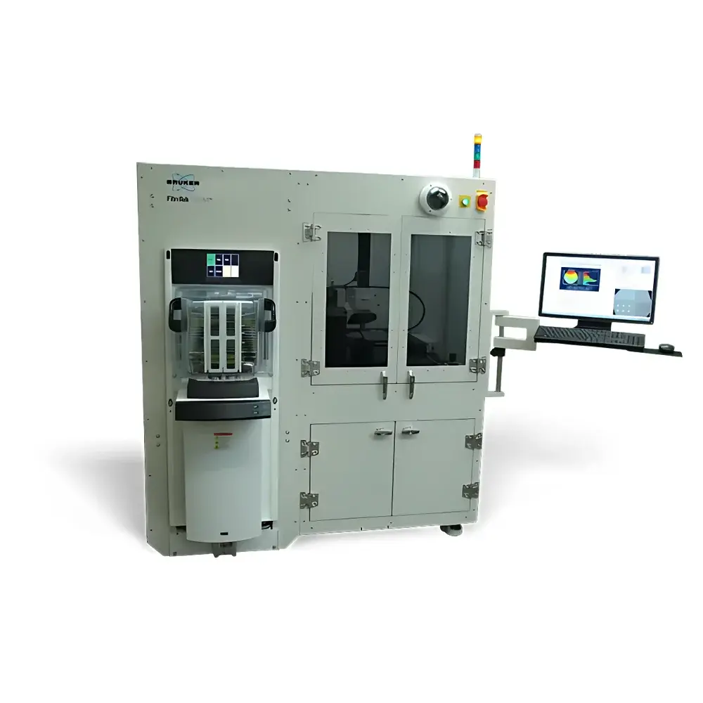
Bruker FilmTek 2000M TSV Ellipsometer
| Brand | Bruker |
|---|---|
| Origin | Germany |
| Manufacturer Type | Authorized Distributor |
| Origin Category | Imported |
| Model | FilmTek 2000M TSV |
| Quotation | Upon Request |
| Sample Size | 200 mm or 300 mm |
| Film Thickness Measurement Accuracy | <0.2% (1σ) |
Overview
The Bruker FilmTek 2000M TSV Ellipsometer is a production-grade, non-contact optical metrology system engineered for high-throughput, high-precision characterization of advanced semiconductor packaging structures. Unlike conventional spectroscopic ellipsometers optimized for thin-film analysis, the FilmTek 2000M TSV employs a proprietary normal-incidence reflectometry architecture—enhanced by ellipsometric modeling—to deliver quantitative depth, height, and critical dimension (CD) measurements on high-aspect-ratio (HAR) features such as through-silicon vias (TSVs), copper pillars, solder bumps, redistribution layers (RDLs), and deep etch trenches. Its optical design integrates low-magnification, low-power objective lenses that produce near-collimated probe beams with spot sizes down to 5 µm × 10 µm (at 10× magnification), enabling spatially resolved measurement across sub-micron-diameter via openings while preserving spectral coherence essential for accurate HAR structure analysis. The system operates on broadband halogen illumination (typically 400–1000 nm) and utilizes a 2048-pixel Sony linear CCD array for high signal-to-noise spectral acquisition, supporting robust fitting of multi-layer optical models under industrial process control constraints.
Key Features
- Simultaneous metrology of TSV etch depth (up to 500 µm), bump height, critical dimension (CD), and film thickness (5 nm – 350 µm) within a single platform
- Normal-incidence reflectometry with ellipsometric modeling—optimized for HAR structures with aspect ratios >10:1
- Sub-micron spatial resolution: configurable spot sizes as small as 5 µm × 10 µm; capable of resolving vias ≥1 µm in diameter
- Measurement repeatability: <0.005% (1σ) for TSV depth and film thickness; <0.2% (1σ) overall film thickness accuracy
- Automated wafer handling: FOUP/SMIF-compatible, 200 mm or 300 mm substrate support; integrated Brooks or SCI robotics interface
- SECS/GEM-compliant communication protocol for factory automation and MES integration
- Measurement speed: ~1 second per data point; throughput >60 wafers per hour (WPH) in production mode
Sample Compatibility & Compliance
The FilmTek 2000M TSV supports bare and patterned silicon wafers (200 mm and 300 mm), including those with dielectric liners (e.g., SiO₂, SiN), metal seed layers (Cu, Ni), and photoresist coatings. It accommodates standard front-end and back-end-of-line (BEOL) packaging substrates, such as interposers, fan-out wafer-level packages (FOWLP), and 2.5D/3D stacked dies. The system complies with SEMI E10 (Specification for Definition and Measurement of Equipment Reliability, Availability, and Maintainability), SEMI E30 (SECS/GEM), and ISO 9001 traceability requirements. Data integrity meets GLP and GMP-aligned audit trail standards—including full operator logging, parameter versioning, and timestamped raw spectrum archiving—supporting FDA 21 CFR Part 11 readiness when deployed with validated software configurations.
Software & Data Management
The system runs on a multi-core Windows 10 platform with Bruker’s proprietary FilmTek Metrology Suite—a modular, scriptable application built for both R&D flexibility and production stability. The software includes automated pattern recognition powered by Cognex VisionPro libraries, enabling robust alignment on sparse or low-contrast TSV arrays. Measurement recipes support multi-site mapping, statistical process control (SPC) charting, and real-time deviation alerts against user-defined tolerance bands. All raw spectra, model parameters, and fit residuals are stored in HDF5 format with embedded metadata (wavelength calibration, stage position, environmental sensor logs). Export options include CSV, XML, and industry-standard SECS-II data streams. Software validation documentation (IQ/OQ/PQ protocols) and change control logs are available upon request for regulated environments.
Applications
- TSV depth and depth uniformity monitoring during Bosch or cryogenic DRIE processes
- Post-plating Cu pillar height and planarity assessment prior to bonding
- RDL line width and sidewall angle quantification on polyimide or BCB dielectrics
- Photoresist thickness mapping across wafer edge and center for lithography process window validation
- Etch stop layer (e.g., TiN, TaN) thickness verification beneath TSV caps
- Non-destructive inline metrology for 3D IC stacking qualification—replacing cross-sectional SEM where throughput or sample preservation is critical
FAQ
What measurement principle does the FilmTek 2000M TSV use?
It combines normal-incidence broadband reflectometry with ellipsometric modeling—leveraging phase and amplitude information from reflected light to extract depth, height, and thickness without physical contact or vacuum requirements.
Can it measure TSVs smaller than 1 µm in diameter?
The standard configuration resolves vias ≥1 µm; sub-µm capability requires optional high-NA optics and is subject to signal-to-noise constraints dependent on material stack and surface roughness.
Is the system compatible with 300 mm FOUPs and automated material handling systems?
Yes—it supports SECS/GEM communication and integrates natively with Brooks and SCI robotic handlers for fully automated cassette-to-cassette operation.
How is measurement uncertainty quantified and verified?
Uncertainty budgets follow ISO/IEC 17025 guidelines; daily verification uses NIST-traceable step-height standards and certified reference wafers; long-term stability is tracked via control charts per SPC methodology.
Does the software support custom optical modeling for novel stack architectures?
Yes—the FilmTek Metrology Suite allows users to define multi-layer optical models using Cauchy, Tauc-Lorentz, or B-spline dispersion functions, with constraint-based fitting for production-grade reproducibility.


