BY2000 Atomic Force Microscope (AFM) – Benyuan Nanotechnology
| Key | Brand: Benyuan Nanotechnology |
|---|---|
| Model | BY2000 |
| Origin | Beijing, China |
| Instrument Type | Atomic Force Microscope (AFM) / Scanning Tunneling Microscope (STM) / Lateral Force Microscope (LFM) |
| Vertical Position Detection Noise | 0.1 nm |
| Maximum Sample Diameter | 45 mm |
| Maximum Sample Thickness | 15 mm |
| XY Sample Stage Travel Range | 100 mm × 100 mm |
| XY Scan Range | ~10 μm |
| Z Scan Range | ~2 μm |
| Image Resolution Options | 128×128, 256×256, 512×512, 1024×1024 pixels |
| Scan Angle | 0–360° |
| Scan Frequency | 0.1–100 Hz |
| Controller | TI 32-bit DSP with Real-Time OS |
| DAC/ADC | 16-bit high-speed |
| High-Voltage Driver | 5-channel APEX integrated HV op-amps |
| Interface | 10/100 Mbps Fast Ethernet |
Overview
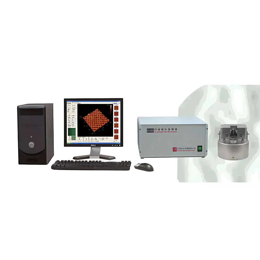
The BY2000 Atomic Force Microscope (AFM), developed by Benyuan Nanotechnology, is a multi-modal scanning probe microscope engineered for high-resolution surface characterization at the nanoscale. Operating on the principle of mechanical force detection between a sharp probe tip and sample surface, the BY2000 supports three primary operational modes: contact-mode AFM, tapping-mode AFM, non-contact AFM, scanning tunneling microscopy (STM), and lateral force microscopy (LFM). Its vertical position detection noise of 0.1 nm enables reliable atomic-scale topographic imaging, while its lateral resolution of 0.2 nm (AFM) and 0.1 nm (STM) meets the stringent requirements of academic nanomaterial research, semiconductor metrology, and advanced thin-film development. The system features a large-sample chamber accommodating specimens up to 45 mm in diameter and 15 mm in thickness—uncommon among benchtop AFMs—making it suitable for heterogeneous samples including wafers, biological substrates, polymer films, and functionalized electrodes. All core control functions are implemented on a Texas Instruments 32-bit digital signal processor (DSP) running a real-time operating system, ensuring deterministic timing for feedback loop execution and synchronized multi-channel data acquisition.
Key Features
- Multi-functional probe platform supporting AFM, STM, and LFM in a single instrument via interchangeable probe holders—no hardware reconfiguration required.
- Full digital control architecture with intelligent recognition of probe type, operational mode, and environmental parameters.
- Automated coarse approach system driven by stepper motors (15 mm travel, 50 nm step resolution), eliminating manual coarse positioning and improving repeatability.
- Integrated five-channel APEX high-voltage operational amplifiers for precise, low-noise Z-scanner actuation across the full 2 µm range.
- Fast Ethernet (10/100 Mbps) interface enabling stable, low-latency communication with host PC—compatible with modern Windows OS environments (XP through Windows 10, via compatibility layer).
- Real-time 3D topographic rendering during scanning, with simultaneous multi-channel signal acquisition (e.g., topography + phase + friction + current) per scan line.
- On-the-fly image reconstruction algorithms including tip shape estimation, tip convolution correction, and known-tip deconvolution for quantitative morphology analysis.
Sample Compatibility & Compliance
The BY2000 accommodates a broad range of conductive and non-conductive samples without requiring metallization or vacuum processing. Its open-stage design allows direct mounting of standard SEM stubs, silicon wafers (up to 3-inch), glass slides, and custom substrates. The 100 mm × 100 mm motorized XY stage enables precise navigation across large-area samples—particularly valuable for mapping heterogeneity in battery electrode coatings, corrosion layers, or printed electronics. While not certified for ISO/IEC 17025 accredited laboratories out-of-the-box, the system’s data integrity features—including timestamped parameter logging, full raw data export (binary and ASCII), and session-based metadata archiving—support GLP-compliant workflows. Software-generated reports include traceable roughness parameters (Ra, Rq, Rz, Sk, Kurtosis) aligned with ISO 4287, ISO 25178, and ASTM E2629 standards.
Software & Data Management
The BY2000 is operated via a native Windows-based software suite offering dual-function modules: real-time instrument control and post-acquisition quantitative analysis. All scan settings—including PID gains, setpoint, scan speed, and trigger thresholds—are saved alongside each image in a structured XML metadata file. Raw datasets (16-bit depth per channel) are stored in vendor-neutral formats compatible with third-party tools such as Gwyddion, MountainsMap, and MATLAB. The software includes automated roughness analysis, particle sizing (with user-definable thresholding and connectivity criteria), cross-sectional profiling, and I–V/I–Z curve fitting for electrical property mapping. Audit trail functionality records operator login, parameter changes, and image export events—facilitating internal QA documentation and alignment with FDA 21 CFR Part 11 principles when deployed in regulated R&D environments.
Applications
- Nanomaterial characterization: graphene flake thickness measurement, CNT dispersion analysis, MOF surface uniformity assessment.
- Semiconductor process control: gate oxide roughness evaluation, CMP endpoint detection, lithography resist profile quantification.
- Biomedical research: collagen fibril periodicity, cell membrane topography under physiological buffers, protein adsorption kinetics on biomaterials.
- Energy materials: SEI layer morphology on cycled Li-ion anodes, catalyst nanoparticle distribution on PEM fuel cell membranes.
- Polymers & coatings: phase separation in block copolymers, scratch resistance mapping, hydrophobic/hydrophilic domain identification via LFM.
FAQ
What operating systems are supported?
The BY2000 software is natively compatible with Windows XP, Windows 2000, and Windows 98; operation on Windows 7/10/11 requires compatibility mode configuration and may necessitate legacy driver signing exemptions.
Is vacuum or inert gas operation possible?
No—the BY2000 is designed exclusively for ambient air and liquid environments; it does not feature vacuum chambers or gas purging ports.
Can the system perform electrical property mapping?
Yes—via conductive-AFM (C-AFM) and scanning tunneling spectroscopy (STS) modes, supporting I–V, I–Z, and dI/dV mapping with synchronized topographic feedback.
What probe types are compatible?
Standard commercial Si and Si₃N₄ cantilevers with reflective coating (for optical lever detection) are supported; STM probes require W or PtIr wire tips with sub-100 nm apex radius.
Is remote technical support available?
Yes—Benyuan Nanotechnology provides toll-free technical assistance (800-number) and maintains service centers in Beijing and Guangzhou for on-site calibration, maintenance, and application training.